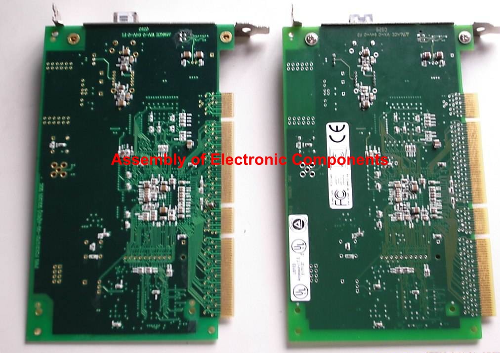
An electricity-controlled device is known as an electronic component. The electronic components are available in a range of shapes and sizes to carry out various electrical operations. So, a wide range of components is used for electronic devices. This article lists a few of the fundamental features related to electronic components and discusses how these characteristics are essential in the assembly of electronic components.
Passive and Active Components
A passive component does not provide any sort of signal gain or power amplification. Examples of passive components may include inductors, resistors, capacitors, and memristors. Since the gain of passive components remains less than one, they cannot intensify or oscillate an input signal. Simply put, a passive device can only multiply an incoming single with a value that is always less than one.
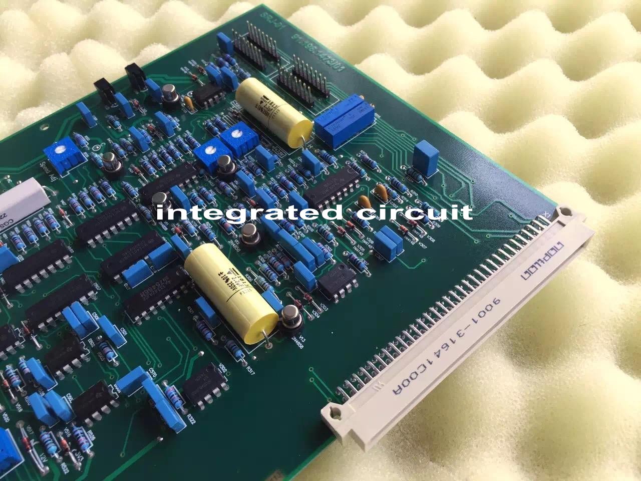
Active components can manipulate input signals by controlling voltage and current levels. They can perform a switching action in the circuit by amplifying and interpreting a signal in various ways. Examples of active components include integrated circuits (ICs), transistors, diodes, and silicon-controlled rectifiers (SCRs). Active electronics components are mainly comprised of semiconductor devices. An active device can have a gain of more than one.
————————————————————-
Request Electronic Contract Manufacturing Quote, Pls Send PCB File to Sales@raypcb.com Now
————————————————————-
Discrete and Integrated Components
An individual component operating independently within a circuit is known as a discrete component. A capacitor is an example of a discrete component; it stores the charge when current passes through it. A discrete component can either be a passive or active device.
Alternatively, an integrated circuit (IC) is created when several discrete components are combined, interconnected in a particular way, and packaged in a specialized enclosure to perform a specific function. Common examples of an IC are microcontrollers, microprocessors, and FPGAs.
Connection Types of the Components
The electronic components can generally be connected to the board in one of two ways, through-hole (TH) components or surface-mount (SM) components. Through-hole components have leads that are inserted in the holes drilled in the PCB. At the same time, SM components are placed directly on the surface of the PCB. High-density integrated circuit assemblies prefer using SM components. High-density IC assemblies are available with pin-grid arrays with many rows of pins located on the component’s bottom. In SM devices, leadless parts are often possible where no metal connectors pop out of the components’ body.
Embedded Components
The PCBs manufacturers are increasingly using embedded components, especially for producing consumer electronics. Mostly the passive components and the ICs are embedded within a PCB. The embedded components can be integrated into wearable devices, and development costs and production loads are projected to be minimized. In particular, there are three embedding approaches to passive components.
Embedding Passive Components makes it possible to embed every currently available part. Since holes in the board are made to carry the materials, the board may get thicker. There is no significant decrease in cost.
Thinner boards are made feasible by embedding advanced thin passive components, and these components may be as thin as 100μm or less. The resin encloses these thin components to securely embed them as the board layers are assembled, virtually eliminating the need for making holes in the board.
The printing of Film components simplifies the packaging stage and reduces the assembly cost because many film components are produced in batches. The circuit’s complexity reduces because the number of solder joints is decreased, providing improved joint durability, compact product, and less environmental impacts.
————————————————————-
Request Electronic Contract Manufacturing Quote, Pls Send PCB File to Sales@raypcb.com Now
————————————————————-
Challenges in Component Assembly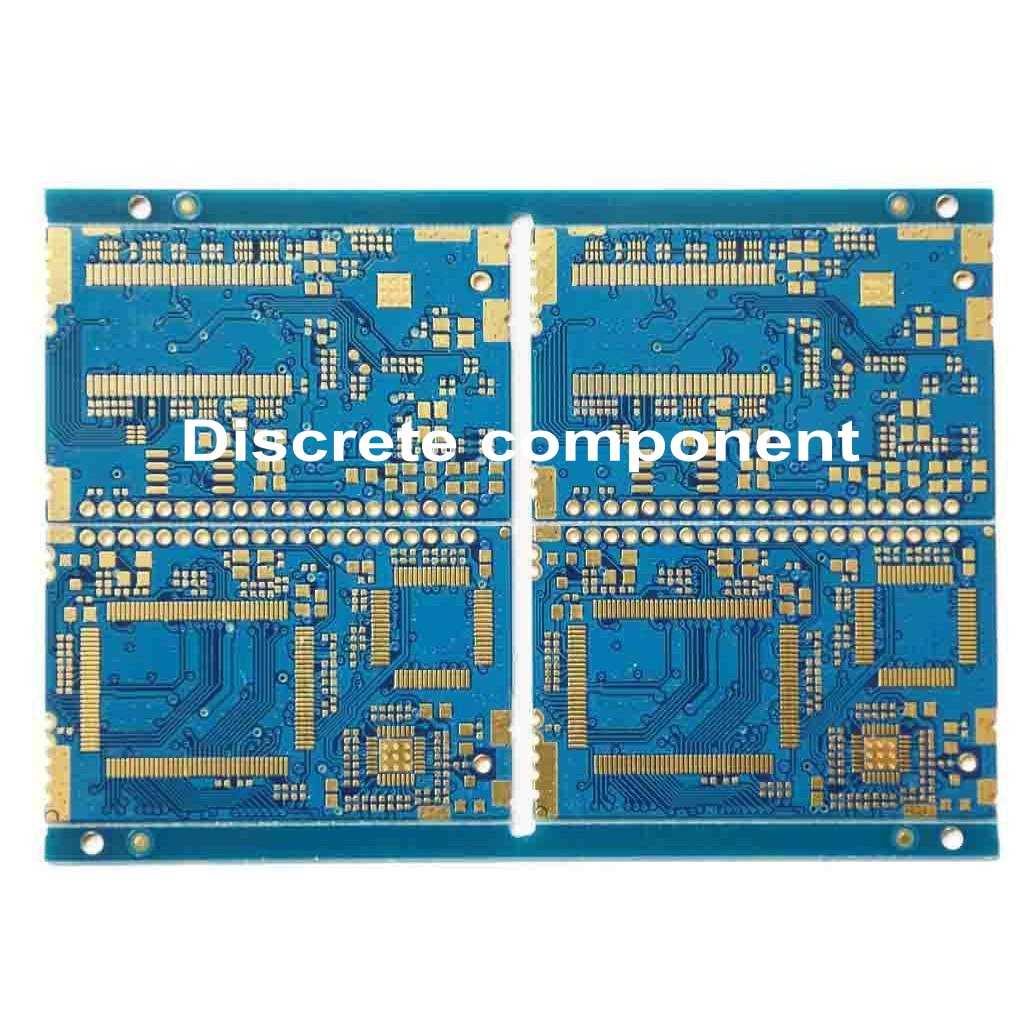
The electronic assembly process has become specialized in recent years. Electronic has become very sophisticated. The primary stages of manufacturing an electronic product are idea, design, plan, and produce. First, the specifications of an idea are laid out, and initial planning is done. Second, the design stage specifies the device functionality. Third, the planning stage involves selecting appropriate components and their position on the board, routing traces to connect different components, and deciding connectors for multiple PCBs.
With the increase in electronic equipment complexity, electronic design automation (EDA) has been developed to assist in the design, manufacturing, and assembly of electronics. Today, electronic products are expected to be more compact, high speed, less power consuming, lightweight, and rich in functionality.
Previously, most circuit boards were used for a single function, such as processor board or power supply board. Meanwhile, every PCB only had a definite role within the overall design; developing and manufacturing were markedly easy. low volume PCB assembly,Through Hole components require wider pin-to-pin distance and relatively greater hole diameter limiting its use in high-density component assemblies.
Pin-to-pin pitches started to shrink with the introduction of surface mounting technologies. The surface-mounted components offered lesser foot-prints and higher pin counts. Trace widths and clearances reduced, making assemblies very compact. With the continued advancement in integration and interconnection, more extensive subsystems can be mounted on an individual chip in a compact package.
A variety of these compact packages can be combined and mounted on a minimal board to produce an incredibly complex intricate system. These days, multiple sections with very different functionality can exist on a single board. These sections may include a GHz RF section, a section for analog and digital components, and a power supply section. PCB designers and manufacturers use ball grid arrays (BGAs) due to their small size, improved performance, and lower power loss. The BGAs are denser than quad flat packages (QFPs), and a micro-packaged μBGA-IC contains thousands of pin-outs.
Using these high-density packages contributes to very dense and complex structures, all crammed together using micro-via and advanced box build technologies on a multi-layer PCB. For component assemblers, PCB designers, and manufacturers, all these specifications present significant challenges.
Process of Electronic Component Assembly
The conventional component assembly approach connects the components with PCBs by inserting their leads into holes in the PCB. The leads are then soldered to the PCB, providing both mechanical support and electrical connection. Later, the surface mount component assembly enabled the utilization of micro-electronics with VLSI IC packages containing huge pin-out numbers. Surface-mount equivalents of all the components are not available, however. So, the PCBs still contain both types of components.
It is possible to manually put together a PCB assembly. However, specialized machines that render the assembly process automated, fast, and secure are more common. Because the final assembly comprises several different kinds of components with different specifications, it is crucial to carefully choose an assembly process based on cost-effectiveness and efficiency. A standard component assembly would contain a range of dual-in-line packages (DIPs), various connectors, and other discrete components such as diodes, capacitors, resistors, and transistors. For their legs to be mounted, all these components have standard hole spacing needed. Simply put, the component assembly process comprises the subsequent phases:
- Collect the components according to the requirements listed in the bill of materials (BOM).
- Get the components ready for placement on the board, e.g., arranging the leads for insertion.
- PCB cleaning by wiping or rinsing in the water using industrial cleaners.
- Recording the measurements of boards and components.
- Placement of components in separate plates in an automated assembly line.
- Placemen of SMT devices and insertion of PTH devices.
- Mass soldering of the components such as reflow soldering.
- Cleaning and Removal of excess flux.
- Placement of heavy or sensitive components can either not survive high soldering temperature or cannot be handled automatically due to their weight.
- Manual Soldering.
- Cleaning Residual Materials.
- Inspection and testing;
- Application of conformal coatings and finishing.
- Storage and warehousing.
This list of different assembling stages is only for reference, and an assembly manufacturer may change the sequence according to the requirements. Depending on the component’s nature, there might be a few occasional variations in the assembly process.
The environment of the Assembly Facility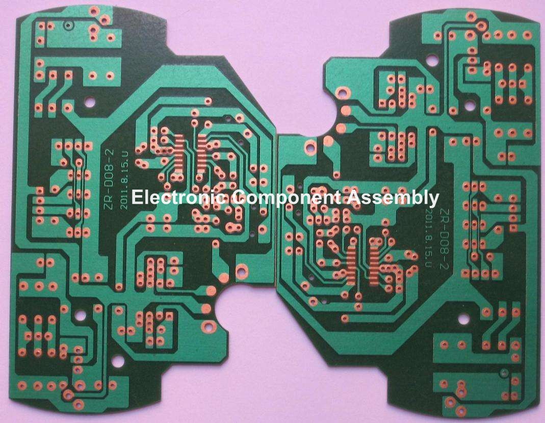
Define the specific electrostatic protected areas in which sensitive parts are handled. To neutralize any positive or negative charges, utilize air ionizers that blast ionized air into the working environment. All goods supplied from vendors must be delivered in sealed conductive containers. The ground resistance, the person, the footwear, and the floor, must not exceed 35 megaohms.
The components, assemblies, and finished products, which are ESD-sensitive, should be labeled with the ESD susceptibility symbol. The ionization produces negative and positive ions drawn to the surface of a charged material, resulting in the neutralization of the charge. The use of suitable packaging materials can protect the product against the charge and reduce the generation of charge caused by any product movement within the enclosure.
It is essential to use anti-static floor material, specifically in the areas where human movement is required. Suitable floor materials may reduce the build-up of charge on furniture and other equipment. ESD-sensitive devices should be labeled with the ESD-susceptible logo. This logo is necessary for all ESD-sensitive systems such as discrete components, ICs, PCBs, and assemblies. Similarly, the objects offering ESD protection must be labeled with the logo of the ESD-protective substance.
Additionally, there are ESD testing apparatus. It is essential for testing but does not provide ESD protection. This apparatus includes footwear indicators, wrist straps, and resistivity meters.
————————————————————-
Request Electronic Contract Manufacturing Quote, Pls Send PCB File to Sales@raypcb.com Now
————————————————————-
Precautions for Handling of Components
When treating parts, the following measures should be observed:
- Sensitive components like ICs must be picked up by the package’s non-conductive area instead of metallic leads. These leads are most susceptible to ESD.
- When handling PCBs, make sure that you touch the board by the edges, avoid solder, and any other conductive surface because some sensitive component may find a path through the conductive surface.
- Remove any non-conductive objects from the workspace to avoid charge-separation in ESD-sensitive components caused by the electric field. Otherwise, the components might be destroyed if it comes into contact with a conductive object in the presence of an electric field.
- Suppose static generating materials are indispensable for the task. In that case, the workplace must be organized to allow more generous spacing between sensitive boards and static generating materials.
- Shoe grounders are necessary for activities performed in standing position, whereas for seated activities, a wrist-strap is advisable. It is also essential to inspect wrist straps and shoe grounders regularly to ensure they are functioning correctly.
Wrist straps used by people seated at work are useful for ESD control. They can be worn securely touching the skin and connected to the common ground. The resistor limits the current by providing a controlled and slow drain of the built-up charge.
Shoe grounders are built to connect the body to a conductive floor or mat via the socks. They are adequate for operations performed in a stand-up position but are not very efficient when seated. The moisture in the socks provides a complete electrical connection to the outside of the socks. There is no need to remove the socks for use with shoe grounders.
Handling of Metal Oxide Semiconductor Components
The human body can generate static charges of about 25,000 volts. These build-ups can discharge through an electrically grounded body or device quickly. The high voltage spike arising from this discharge destroys the terminals of ICs. Moving humans, low humidity, insufficient grounding, unshielded wires, weak joints, and moving equipment are the most frequent electrostatic discharge sources (ESD).
ESD of 10,000-25,000 Volts is not detrimental to human beings. Instead, one ampere current at 230 Volts mains power supply is fatal. The current supplied by ESD voltages are only in the range of micro-amperes, which is not hazardous for human beings. The human body’s static electricity is strong enough to destroy a complementary metal-oxide-semiconductor (CMOS) if you hit CMOS input pins with your fingertips.
A grounding harness should be attached to the ground by the individual holding MOS equipment. During the handling of high voltage components, like power supplies, anti-static straps must not be worn. Anti-static mats constructed with rubber or any other anti-static substances should be used in the work areas. After installation of all other components, place MOS IC on the boards. The PCB terminals should have conductive clips or tape mounted on them.
It is required that workers operating MOS equipment wear anti-static clothes. Workplace tabletops and trays must be non-conductive. The soldering iron should be grounded. When the power is ON, do not connect or disconnect the MOS device from test sockets. Voltage surges often occur due to the switching of relays. If the device’s power supply is off, signals must not be applied to the device’s input terminals. New MOS terminals must be attached to either the ground or supply voltage.
Comments are closed