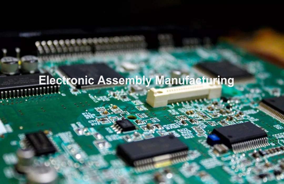
Electronic devices are a mixture of linked electrical and electronic parts to establish a specifically designed purpose. In the early days, the electronic equipment was assembled by wiring manually or by soldering in a point-to-point method. Later, with the introduction of smaller electronic parts, replaceability enhanced, modular architecture became common, and the time it took to manufacture electronics assembly reduced considerably. Furthermore, due to increased replaceability, it becomes easy to repair malfunctioned equipment.
The PCB establishes the physical basis for the assembly of electronic components and the electrical link between the various parts. For utilizing printed circuit boards, there are several valid reasons, some of which are as follows:
With a related reduction in weight, the scale of the device assembly is decreased. The positioning of components is set, making it simpler to locate and manage electronic devices and systems. Minimal technological expertise and preparation are needed by PCB repairing staff. Incorrect or short-circuited wiring incidents can be reduced.
————————————————————-
Request Electronic Contract Manufacturing Quote, Pls Send PCB File to Sales@raypcb.com Now
————————————————————-
Development in the Manufacturing of PCBs
Dr. Paul Eisler is also considered the Founder of the technology of printed circuit boards. He recommended copper coated insulation material in the form of a sheet as a base material for PCB production. His research gives rise to an industrial manufacturing system and a PCB electronic assembly technique.
Over time, new processes such as photo film lamination, solder masking with solder paste, film resist, legend printing, and CNC drilling has been introduced in electronic assembly manufacturing. The development of multilayer and rigid-flexible PCBs decreased board size dramatically. This was made possible due to advancements in blind and buried vias, plated-through-hole (PTH) interconnections, and wet chemical processes. Advancements in surface mount technology have contributed to a range of developments in PCB materials and procedures, and there is a continuous demand for further improvement in PCB technology.
The assembly manufacturers require integrated circuits (ICs) with even more capacity. High density interconnects structures (HDIS) is made possible by increasing the number of input-output (I / O) terminals of the ICs. Now a large number of companies are producing HDIS. High-frequency devices perform high-speed tasks. These high-frequency PCB assemblies demand the electrical losses to be kept at a minimum.
For electronic manufactured products, PCBs have become an essential aspect. Therefore, the electronic manufacturing industry is on the rise globally. Likewise, by more carefully regulated cost-effective methods, the electronic manufacturing industry will continue to offer higher functionality with higher density, reduced cost, and improved reliability. The usage of flexible circuits is projected to grow much further. Demand is increasing for the manufacturing of environment-friendly lead-free PCBs. The different forms of PCBs, both those already in operation and those to be produced, are likely to maintain their role as an integral component of electronics assembly.
————————————————————-
Request Electronic Contract Manufacturing Quote, Pls Send PCB File to Sales@raypcb.com Now
————————————————————-
Types of PCBs in Assembly Manufacturing
Printed Circuit Boards can be grouped according to their distinctive features and characteristics. The introduction of surface mount technology and the advancement of autonomous assembly techniques demand that the boards must be produced to stringent mechanical tolerances, even for the product that is low cost. A simplified and more comprehensible classification is used for PCBs, which is defined by two general parameters: one is the number of planes or layers that contain connection tracks, and the other is the existence or absence of plated-through-holes. It is simple to categorize PCSs by inherent characteristics of the boards. Below, the essential types of PCBs are mentioned.
Single-sided PCBs
Connection tracks are on one side of the substrate in a single-sided PCB. The side with tracks is known as the solder side, while the side contains the components, therefore known as the component side. In the manufacture of basic electronic instruments, single-side PCBs are used to keep the costs down. The single-sided PCBs are developed primarily by the process called printing and etching or by the die-cut method. In this method, the pattern of interconnected tracks is photo-engraved or machine-engraved on a die.
Double-sided PCBs
This type of PCB has connection tracks on both sides of the substrate. Double-sided PCBs have two variants, one with PTH, another without PTH. Double-sided PTH PCB has copper traces on two sides of a laminated substrate. The metallic wall of the hole connects two sides of the board. These kinds of boards are useful for high-density complex assemblies. These boards are significantly cost-effective. For plated through holes, various kinds of eyelets can be used for interconnections.
Multi-Layer PCBs
Multilayer PCBs combine two or more boards with a thin layer of resin-impregnated material sandwiched between each layer. Multi-layer PCBs have more than three layers. The multilayer PCB is used in circumstances where the required connection density is substantial. The multiple layers of the PCB contain high capacitance offering a robust decoupling for power supply, enabling high-speed circuits to work satisfactorily. The interior layers can be used for interconnections, and a thick, strong copper heat sink can be placed on external surfaces. It is possible to manufacture four-layer and six-layer boards with about the same simplicity as double-sided boards. Based on the complexity and the equipment used, the expense of a printed circuit board varies. Multilayer boards are no longer confined to just high-tech items; instead, their use has become widespread.
Rigid-Flex PCBs
Rigid-flex boards are mostly made up of multiple individual boards. They are three-dimensional assemblies that are flexibly connected. The rigid-flex boards enable high-density packaging. Flexible PCB assemblies may contain boards that are single-sided, double-sided, or multi-layered. Typically, very thin, the base material is in the region of 0.1 mm thickness.
————————————————————-
Request Electronic Contract Manufacturing Quote, Pls Send PCB File to Sales@raypcb.com Now
————————————————————-
Manufacturing of PCB Assembly
Most of the electronic assembly manufacturing processes have identical or similar necessary steps. The print and etch technique, a strictly subtractive method, is the most common PCB manufacturing procedure. Alternatively, there is an additive process called printed wiring. In this method, connection tracks are printed on the laminate using conductive material to connect components.
There is a need to consider four primary stages of the PCB assembly production process. This involves designing, production, assembly, and final testing. Following innovations in software-based development and testing procedures, the increasing sophistication of printed circuit boards lets the circuit designer look past the individual component technique. The following steps represent the design and fabrication process of PCBs.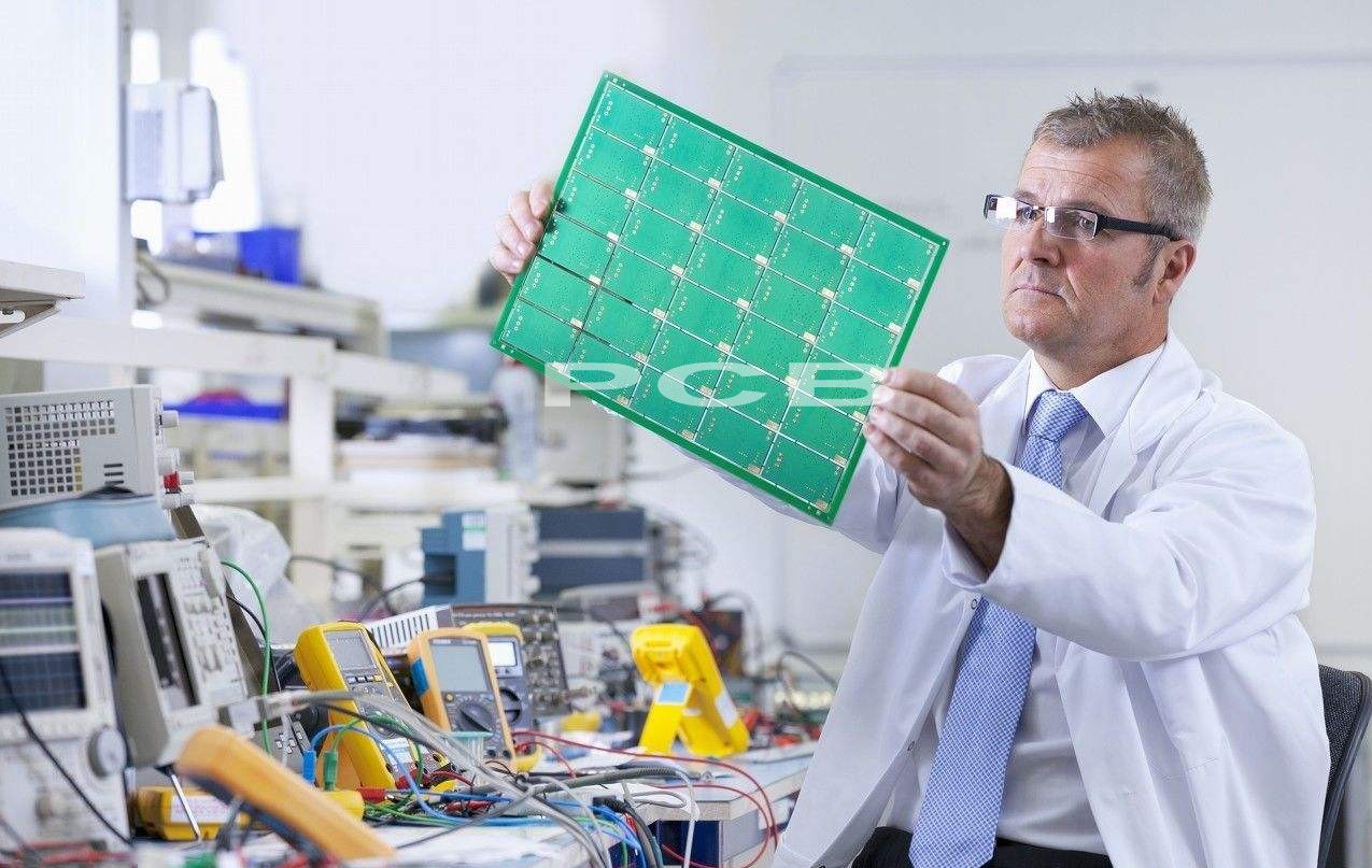
Circuit Diagram
Circuit diagrams provide information about all the electronic parts and how they are connected. There are various circuit simulation applications. Using these applications, a circuit design can be thoroughly tested before being finalized. All the limitations of a circuit are analyzed before being sent to the PCB designing program. An efficient design must include all the crucial data essential for understanding the operation of the circuit. The simulation program and PCB designing program work simultaneously to ensure the design is printed completely.
Generating Designs
The circuit schematic diagram is used as a reference for the identification of electronic components and layout connections. To enhance accuracy, the resolution of the design layout is increases multiple times. However, the final printing of the design is done according to the actual measurements. The print is taken either in the form of positive or negative engraving, based on the equipment kind and the assembly suppliers’ preference. The initial PCB design would go on to define the final physical form of the end product.
Board Manufacturing
A typical PCB is made up of copper-clad substrate board; generally, the copper is on one side of the board. The laminated sheets are appropriately cut to make required sized boards. The most frequently used substrate or base material is known as FR-4. It is an all woven glass laminated epoxy. It is generally 1.6 mm thick with a copper layer of 305 grams per square meter. The copper thickness is around 35 microns. The mechanical characteristics of FR4 include improved strength against punching and drilling, enhanced flexibility, and fire and water resistance.
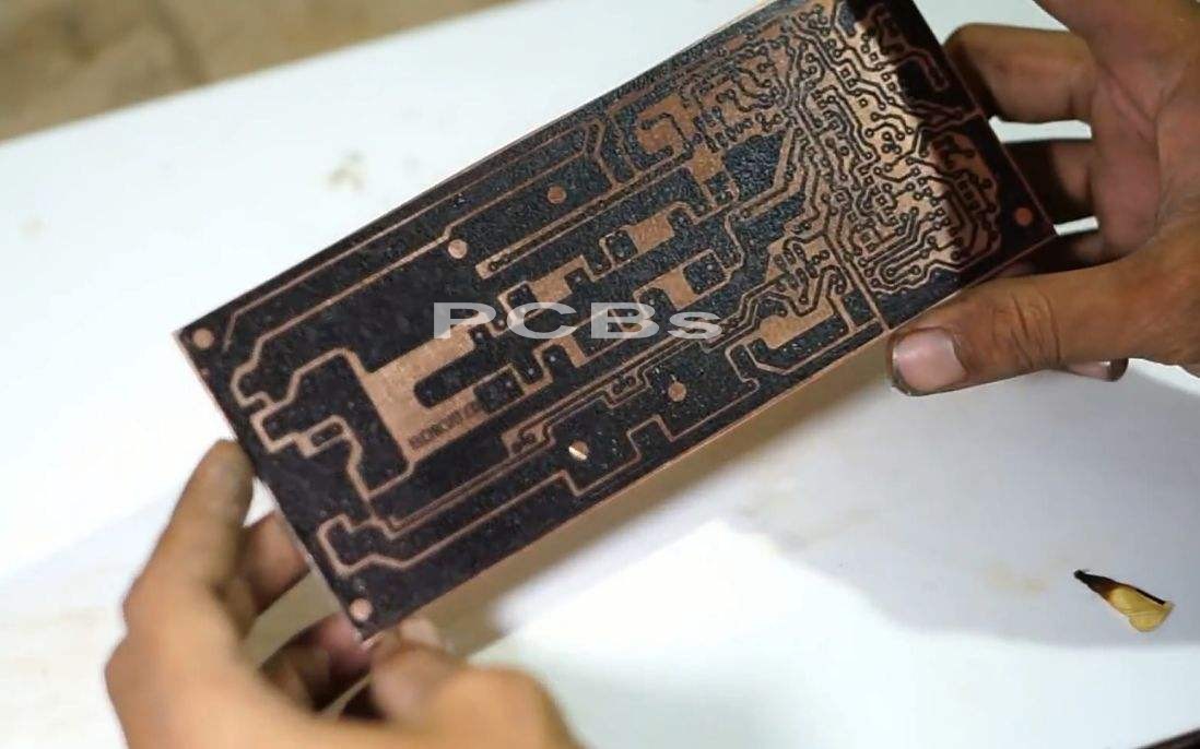
Transfer of Design
The next stage in the electronics assembly manufacturing is to transfer the circuit’s initial design on the copper-clad PCB surface. The design could be transferred using a stenciling technique. The ink that serves as an etch-resist covers the copper that is needed to be kept after etching. Screen printing is limited to low precision image transfer with less strict design specifications in current PCB manufacturing facilities. A safer approach is to use a photoresist dry film susceptible to ultraviolet light (200-500 nm). The dry film is heated and placed on the board’s copper side. The resist’s development is carried out, allowing certain parts of copper to be maintained on the boards that were covered by a resist.
Etching
The essence of the electronic PCB assembly production is the etching process. To obtain intended circuit patterns, etching is performed to scrape off the copper from unwanted places. Ferric chloride is the oldest and most widely used etching substance, which oxidizes copper to form cuprous chloride. The immersion, bubble, splash, or spray technique is typically used for etching. The spray etching process is the most widespread and is pumped in high pressure from a container to the nozzles.
————————————————————-
Request Electronic Contract Manufacturing Quote, Pls Send PCB File to Sales@raypcb.com Now
————————————————————-
Drilling of Holes
Typically, mass manufacturing employs numerically operated drilling machines with multiple heads. To ensure the proper drill sizes are used, and no holes have been left out, jigs are used. On fiberglass boards, tungsten carbide or diamond-tipped drills are favored. The size of electronic components has dramatically declined in recent years. The requirement for even smaller hole diameters has increased due to the reduction in the size of electronic devices
Coatings and Finishes
Copper has superior electric conductivity characteristics with higher thermal stability. PCBs use some finishing materials for surface coatings. Generally, the surface finish is applied to shield the exposed copper tracks and pad against corrosion and other wear and tear. The coating helps ensure that the board can be soldered without damaging other components during assembly. Typically, the standard process of PCB production involves the protection of circuit traces with a masking agent called a solder mask. This solder mask is removed once the process of soldering begins. A surface finishing method would shield the areas that are not protected with a solder mask. The application of solder made from tin or lead to bare copper results in a chemical bond that prevents oxidation. Subsequently, the PCB is immersed in a nitrogen solution that is not absorbed by the laminate; instead, it adheres to exposed metal surfaces.
Testing of Assemblies
The assembled PCBs can be tested in several ways. Bare board test and loaded board tests are two essential checks for testing PCBs. Bare board test is used for detecting any shorts between tracks and open tracks. Loaded board tests’ primary function is to analyze the defects that may have arisen during the manufacturing process. Loaded board tests also involve various other in-circuit functionality tests. The frequency of failure in dense PCBs can reach up to 20 percent; it has been noticed. In electronic assembly manufacturing, bare board checking has become mandatory.
There is an alternative additive method for manufacturing printed circuit boards in addition to the widely used printing and etching technique. There’s no copper on the substrate in this process. The copper is systematically deposited on the base laminate wherever desired, as per the circuit design.
The procedure is more complicated for the creation of double-sided PTH boards than the printing and etching system. By dipping the PCB in a stannous chloride solution, the board is sensitized then it is immersed in an acidified solution of palladium chloride. A solution of copper sulfate, sodium hydroxide, formaldehyde, and some reducing agent and additives is used for Electroless copper deposition on the holes’ walls. With the resist separated from the region where the traces are kept, the design transfer mechanism happens. The Reinforced Photoresist protects all other regions. Subsequently, after immersing the board in an electroplating solution, the uncovered track areas are electroplated with tin-lead Alloy. All conductors required on the PCB and within the holes get plated. Finally, the surface finishing is done by coatings techniques including and not limited to solder masking, hot-air leveling, and surface protection using organic substances.
Multi-layered PCBs are manufactured by combining undrilled pre-etched copper-clad substrates. Individual panels are sandwiched together s. the combined stack is laminated to create a single multilayer board.
Comments are closed