SMD prototype PCBs are a crucial component in the development of modern electronics. These small, lightweight boards are used to prototype and test new designs before they go into production. SMD, or surface mount technology, is a method of electronic component placement that allows for smaller and more densely packed circuitry. This makes SMD prototype PCBs ideal for use in portable devices, such as smartphones and tablets, as well as in other applications where space is at a premium.
SMD prototype PCBs offer a number of advantages over traditional through-hole PCBs. For one, they are much smaller and more compact, which means that they can be used in a wider range of devices. Additionally, SMD components are typically less expensive than their through-hole counterparts, which can help to reduce the overall cost of production. Another advantage of SMD prototype PCBs is that they are much easier to assemble and solder, which can save time and reduce the risk of errors during the manufacturing process.
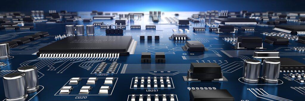
What is an SMD Prototype PCB?
An SMD Prototype PCB, or Surface Mount Device Prototype Printed Circuit Board, is a type of PCB that is used to create small-scale electronic prototypes. SMD Prototype PCBs are designed to be compact, lightweight, and easy to use. They are used by engineers, hobbyists, and DIY enthusiasts to create electronic circuits for a wide range of applications.
SMD Prototype PCBs are made using surface mount technology, or SMT. This technology involves mounting electronic components directly onto the surface of the PCB, rather than inserting them through holes in the board. This allows for a more compact and efficient design, as well as faster production times.
SMD Prototype PCBs are typically used for small-scale projects, such as those involving microcontrollers, sensors, and other electronic components. They are also used for prototyping larger projects, as they allow engineers to test their designs before moving on to larger-scale production.
Overall, SMD Prototype PCBs are an essential tool for anyone working in the field of electronics. They are easy to use, efficient, and versatile, making them ideal for a wide range of applications.
Advantages of SMD Prototype PCBs
Smaller Size
SMD (Surface Mount Device) technology allows for smaller components and a more compact design. This means that SMD prototype PCBs take up less space and can be used in smaller electronic devices. The small size of SMD components also allows for more components to be placed on a single board, increasing the functionality of the device without increasing its size.
Cost-Effective
SMD prototype PCBs are cost-effective due to the smaller size of the components and the ability to automate the assembly process. SMD components are less expensive to manufacture and can be placed on the board using automated pick-and-place machines, reducing labor costs. Additionally, SMD prototype PCBs require less material and are easier to transport, further reducing costs.
Faster Production Time
SMD prototype PCBs can be produced faster than through-hole PCBs due to the automated assembly process. The pick-and-place machines can place components on the board at a much faster rate than manual assembly, reducing production time. Additionally, SMD components can be placed on both sides of the board, allowing for more components to be placed in a smaller space and reducing the need for multiple boards.
In summary, the advantages of SMD prototype PCBs include smaller size, cost-effectiveness, and faster production time. These benefits make SMD technology a popular choice for electronic devices that require a compact design, high functionality, and efficient production.
Design Considerations for SMD Prototype PCBs
Component Placement
When designing an SMD prototype PCB, proper component placement is crucial. It is important to consider the size and orientation of the components, as well as their proximity to one another. This can greatly affect the performance and reliability of the PCB.
One important factor to consider is the placement of decoupling capacitors. These capacitors should be placed as close as possible to the power and ground pins of the component they are decoupling to minimize the inductance of the power and ground traces.
Another consideration is the placement of high-speed components, such as microcontrollers and memory chips. These components should be placed as close as possible to each other to minimize the length of the signal traces and reduce the potential for signal degradation.
Trace Width and Spacing
The width and spacing of traces on an SMD prototype PCB can also greatly affect its performance. It is important to ensure that the traces are wide enough to handle the current they will be carrying, and that there is enough spacing between them to prevent crosstalk and other signal integrity issues.
When designing traces for high-speed signals, it is important to consider the characteristic impedance of the trace. This can be achieved by using a trace width calculator to determine the appropriate trace width for the desired impedance.
Signal Integrity
Signal integrity is a critical consideration when designing an SMD prototype PCB. It is important to ensure that the signal traces are properly routed to minimize signal degradation and crosstalk.
One way to achieve this is by using differential pairs for high-speed signals. This can greatly improve signal integrity and reduce the potential for electromagnetic interference (EMI) and radio frequency interference (RFI).
Thermal Management
Thermal management is also an important consideration when designing an SMD prototype PCB. It is important to ensure that the PCB can dissipate heat effectively to prevent overheating and component failure.
One way to achieve this is by using thermal vias to transfer heat from the components to the ground plane. It is also important to ensure that components are not placed too close together, as this can lead to thermal issues.
Overall, careful consideration of these design considerations can greatly improve the performance and reliability of an SMD prototype PCB.
| Design Considerations | Importance |
|---|---|
| Component Placement | High |
| Trace Width and Spacing | High |
| Signal Integrity | High |
| Thermal Management | Medium |
Manufacturing Process for SMD Prototype PCBs
PCB Design
The first step in the manufacturing process for SMD prototype PCBs is designing the PCB layout using software such as Eagle, Altium, or KiCAD. The design should take into consideration the size, shape, and number of layers of the PCB. It should also include the placement of SMD components, their footprints, and the routing of traces.
Solder Paste Stenciling
After the PCB design is finalized, a stencil is created using a laser cutter or a chemical etching process. The stencil is used to apply solder paste to the PCB, which is necessary for attaching SMD components to the board. The solder paste is applied through the stencil using a squeegee or a stencil printer.
Component Placement and Soldering
Once the solder paste is applied, SMD components are placed on the board using a pick and place machine or by hand. The components are then soldered to the board using a reflow oven or a hot air gun. The reflow oven melts the solder paste, which creates a permanent connection between the components and the board.
Testing and Inspection
After the soldering process is complete, the PCB is tested and inspected for any defects. This includes checking for short circuits, open circuits, and incorrect component placement. Automated optical inspection (AOI) machines are commonly used for this purpose, as they can quickly detect any defects that may have been missed during manual inspection.
Overall, the manufacturing process for SMD prototype PCBs requires careful attention to detail and a thorough understanding of the design and assembly process. With the right tools and expertise, however, it is possible to create high-quality SMD prototype PCBs that meet the needs of a wide range of applications.
Applications of SMD Prototype PCBs
Consumer Electronics
SMD prototype PCBs are widely used in consumer electronics. They are used in smartphones, tablets, laptops, and other electronic devices that require high-density interconnects. SMD prototype PCBs are also used in gaming consoles, smart TVs, and other entertainment devices. They are preferred over through-hole PCBs due to their small size, lightweight, and high reliability.

Automotive Industry
SMD prototype PCBs are also extensively used in the automotive industry. They are used in electronic control modules, engine control units, and other safety-critical systems. SMD prototype PCBs are preferred over through-hole PCBs due to their ability to withstand high temperatures, vibrations, and shock. They also offer high-density interconnects, which are essential for modern automotive systems.
Medical Devices
SMD prototype PCBs are used in medical devices such as pacemakers, insulin pumps, and other implantable devices. They are also used in diagnostic equipment such as ultrasound machines, CT scanners, and MRI machines. SMD prototype PCBs are preferred over through-hole PCBs due to their small size, lightweight, and high reliability. They also offer high-density interconnects, which are essential for miniaturization in medical devices.
Industrial Automation
SMD prototype PCBs are used in industrial automation systems such as programmable logic controllers (PLCs), human-machine interfaces (HMIs), and other control systems. They are preferred over through-hole PCBs due to their small size, lightweight, and high reliability. SMD prototype PCBs also offer high-density interconnects, which are essential for miniaturization in industrial automation systems.
In conclusion, SMD prototype PCBs are widely used in various industries due to their small size, lightweight, high reliability, and high-density interconnects. They are preferred over through-hole PCBs in many applications due to their superior performance and functionality.
Comments are closed