Custom PCB printing and assembly is a critical aspect of electronics manufacturing. PCBs or Printed Circuit Boards are the backbone of modern electronics, and their design and assembly are crucial to the functionality of electronic devices. PCBs are used in almost every electronic device, from smartphones and laptops to cars and medical equipment.
Custom PCB printing and assembly is the process of designing and manufacturing printed circuit boards according to specific requirements. This process involves designing the circuit board layout, selecting the appropriate components, and assembling the board. Custom PCB printing and assembly is essential for companies that require unique PCB designs that cannot be found in off-the-shelf products. This process allows manufacturers to create unique PCBs that are tailored to their specific needs and requirements.
Custom PCB Printing
What is Custom PCB Printing
Custom PCB printing is the process of creating a printed circuit board (PCB) that is tailored to a specific application. This involves designing a circuit board with specific dimensions, layout, and components to meet the needs of a particular project. Custom PCB printing is typically used in industries such as aerospace, medical, and automotive where reliability and precision are critical.
Benefits of Custom PCB Printing
Custom PCB printing offers several benefits over off-the-shelf PCBs. These include:
- Improved precision and accuracy
- Increased reliability
- Reduced costs
- Faster turnaround time
Custom PCBs can be designed to meet the exact specifications of a project, resulting in a more precise and accurate product. This can lead to increased reliability and reduced costs in the long run. Additionally, custom PCBs can be produced faster than off-the-shelf PCBs, allowing for quicker prototyping and product development.
Types of Custom PCB Printing
There are several types of custom PCB printing, including:
- Single-sided PCBs
- Double-sided PCBs
- Multi-layer PCBs
- Flexible PCBs
Single-sided PCBs are the simplest type of custom PCB and are ideal for simpler electronic devices. Double-sided PCBs have two layers of copper, allowing for more complex circuits. Multi-layer PCBs have multiple layers of copper and are ideal for more complex devices. Flexible PCBs are designed to be flexible, allowing for more compact and lightweight devices.
Overall, custom PCB printing offers several benefits over off-the-shelf PCBs and is an essential tool for many industries that require precision and reliability in their electronic devices.
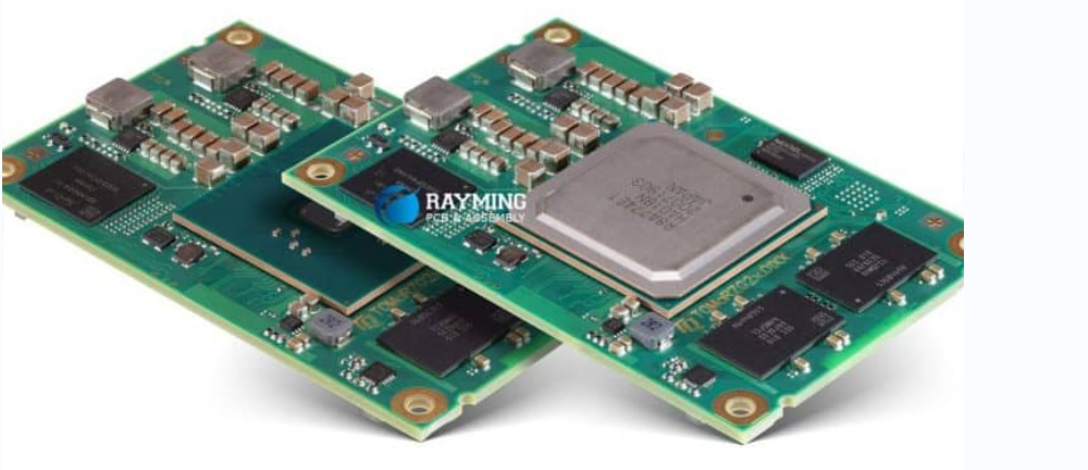
PCB Assembly
What is PCB Assembly?
PCB assembly is the process of attaching electronic components to a printed circuit board (PCB). The PCB is designed to connect and control electronic devices by providing a path for electrical signals. PCB assembly involves placing components on the board and soldering them in place.
Benefits of PCB Assembly
PCB assembly offers several benefits, including:
- Reduced assembly time: PCB assembly can reduce the time required to assemble electronic devices, as the components are already attached to the board.
- Improved reliability: PCB assembly ensures that components are properly connected and secured in place, reducing the risk of failure or malfunction.
- Cost savings: PCB assembly can reduce the cost of assembling electronic devices, as it eliminates the need for manual component placement and reduces the risk of errors.
Types of PCB Assembly
There are two main types of PCB assembly:
-
Through-hole assembly: In this type of assembly, components are inserted into holes drilled in the PCB and soldered in place. Through-hole assembly is typically used for larger components and for applications where reliability is critical.
-
Surface mount assembly: In this type of assembly, components are mounted directly onto the surface of the PCB and soldered in place. Surface mount assembly is typically used for smaller components and for applications where space is limited.
PCB assembly can be done manually or using automated equipment. Automated assembly is faster and more precise, but manual assembly may be necessary for certain components or applications.
Overall, PCB assembly is an important process in the manufacturing of electronic devices, offering improved reliability, reduced assembly time, and cost savings.
Custom PCB Printing and Assembly Services
What are Custom PCB Printing and Assembly Services
Custom PCB printing and assembly services are a type of service that allows businesses and individuals to design and manufacture printed circuit boards (PCBs) that are tailored to their specific needs. These services typically include the design, printing, and assembly of PCBs, as well as testing and quality control to ensure that the final product meets the customer’s specifications.
Benefits of Custom PCB Printing and Assembly Services
Custom PCB printing and assembly services offer a range of benefits to businesses and individuals who need high-quality, customized PCBs. Some of the key benefits include:
-
Flexibility: Custom PCB printing and assembly services allow businesses and individuals to design and manufacture PCBs that meet their specific needs, rather than relying on generic off-the-shelf solutions.
-
Cost-effectiveness: By working with a custom PCB printing and assembly service provider, businesses and individuals can often save money compared to purchasing pre-made PCBs.
-
Quality control: Custom PCB printing and assembly service providers typically have strict quality control measures in place to ensure that the final product meets the customer’s specifications and is of high quality.
How to Choose a Custom PCB Printing and Assembly Service Provider

When choosing a custom PCB printing and assembly service provider, it is important to consider a range of factors, including:
-
Experience: Look for a provider with a proven track record of delivering high-quality custom PCBs.
-
Technology: Choose a provider that uses the latest technology and equipment to ensure that your PCBs are of the highest quality.
-
Customer service: Look for a provider that offers excellent customer service and support throughout the design and manufacturing process.
-
Pricing: Compare pricing from different providers to ensure that you are getting a fair price for the services you need.
Overall, custom PCB printing and assembly services offer a range of benefits to businesses and individuals who need high-quality, customized PCBs. By choosing the right service provider, you can ensure that your PCBs are designed and manufactured to your exact specifications, and that they meet the highest standards of quality and reliability.
Factors to Consider When Designing a Custom PCB
When designing a custom PCB, there are several factors that you need to consider to ensure that your final product meets your requirements. Here are some of the main factors to keep in mind:
Size and Shape
The size and shape of your PCB will depend on the size of the device it will be used in. You should consider the available space and the required components when deciding on the size and shape of your PCB. A small PCB may be suitable for a wearable device, while a larger PCB may be necessary for a complex electronic device.
Number of Layers
The number of layers in your PCB will depend on the complexity of your circuit. A simple circuit may require only one or two layers, while a more complex circuit may require four or more layers. Keep in mind that the more layers you have, the more expensive your PCB will be.
Materials Used
The materials used in your PCB will affect its performance and durability. You should choose materials that are suitable for your application and environment. FR-4 is a common material used in PCBs, but there are other options available, such as ceramic and metal core PCBs.
Circuit Complexity
The complexity of your circuit will affect the layout of your PCB. You should consider the placement of components and the routing of traces to ensure that your circuit operates correctly. A complex circuit may require a more detailed layout, while a simple circuit may be easier to design.
PCB Testing
Testing is an important part of the PCB design process. You should consider how you will test your PCB to ensure that it is functioning correctly. You may need to perform electrical testing, functional testing, or environmental testing to ensure that your PCB meets your requirements.
In conclusion, designing a custom PCB requires careful consideration of several factors, including size and shape, number of layers, materials used, circuit complexity, and PCB testing. By taking these factors into account, you can ensure that your final product meets your requirements and performs as expected.
How to Design a Custom PCB
PCB Design Software
To start designing a custom PCB, you will need to choose the right PCB design software. There are many options available, both free and paid. Some popular choices include Eagle PCB, Altium Designer, and KiCAD. It’s important to choose a software that suits your needs and skill level.
Schematic Capture
Once you have chosen your PCB design software, the next step is to create a schematic. This is a graphical representation of the circuit you want to build. You can use the software’s schematic capture tool to create the schematic. It’s important to ensure that the schematic is accurate and complete.
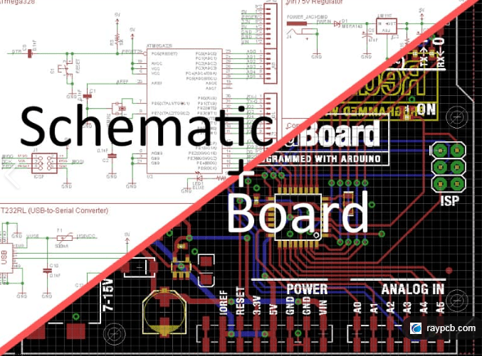
PCB Layout
After creating the schematic, the next step is to design the layout of the PCB. This involves placing the components on the board and connecting them with traces. The software’s PCB layout tool can help you with this. It’s important to ensure that the layout is optimized for the circuit’s performance and that there are no errors.
Component Placement
When placing the components on the board, it’s important to consider factors such as size, shape, and orientation. You should also ensure that there is enough space between the components to avoid interference. The software’s component placement tool can help you with this.
Routing
Routing involves connecting the components with traces on the PCB. You should ensure that the traces are of the right width and thickness and that they follow the shortest path. The software’s routing tool can help you with this.
By following these steps, you can design a custom PCB that meets your requirements.
Comments are closed