Circuit board layout design is a critical aspect of electronic product development. It involves the placement of components and the routing of electrical connections on a printed circuit board (PCB). The layout design can affect the performance, reliability, and cost of the final product.
A well-designed circuit board layout can improve the performance of the electronic circuit by minimizing noise, reducing signal distortion, and optimizing signal integrity. It can also reduce the risk of electrical interference and improve the product’s reliability. Furthermore, a well-designed layout can reduce the manufacturing cost by minimizing the number of layers required and optimizing the use of available space.
The Basics of Circuit Board Layout Design
Understanding the Purpose of Circuit Board Layout Design
The purpose of circuit board layout design is to create a physical representation of an electronic circuit. Circuit board layout design involves arranging electronic components on a printed circuit board (PCB) in a way that meets the electrical and mechanical requirements of the circuit. The layout must also be optimized for manufacturing, testing, and cost-effectiveness.
Components of a Circuit Board Layout Design
A circuit board layout design consists of the following components:
-
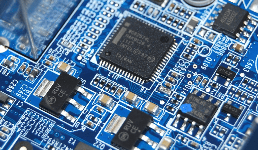
Components: These are the electronic parts that make up the circuit, such as resistors, capacitors, and integrated circuits.
-
Traces: These are the conductive paths that connect the components on the PCB.
-
Pads: These are the areas on the PCB where the components are soldered.
-
Vias: These are the holes in the PCB that allow the traces to pass through from one layer to another.
-
Silkscreen: This is the labeling on the PCB that identifies the components and their placement.
Types of Circuit Board Layout Design
There are two main types of circuit board layout design: single-sided and double-sided. Single-sided PCBs have components and traces on only one side of the board, while double-sided PCBs have components and traces on both sides of the board. Double-sided PCBs are more complex and expensive to manufacture, but they allow for more compact designs and can handle more complex circuits.
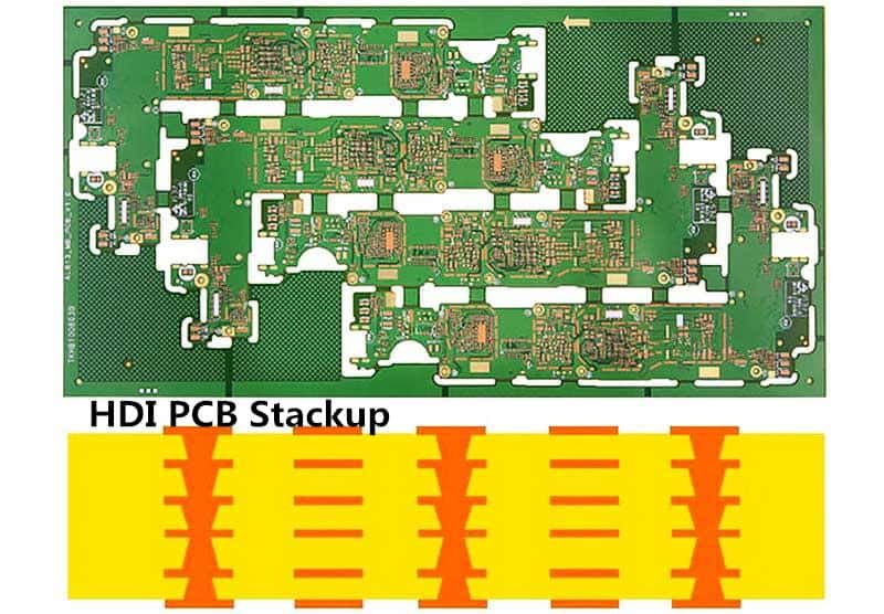
In addition to single-sided and double-sided PCBs, there are also multi-layer PCBs, which have multiple layers of conductive material sandwiched between layers of insulating material. Multi-layer PCBs are used for complex circuits that require a high degree of precision and reliability.
Overall, circuit board layout design is a crucial part of electronic circuit design and requires careful consideration of the electrical, mechanical, and manufacturing requirements of the circuit.
Design Considerations for Circuit Board Layout
When designing a circuit board, there are several key considerations that need to be taken into account. These include signal integrity, power integrity, electromagnetic interference, and thermal management.
Signal Integrity
Signal integrity is critical for ensuring that the circuit operates correctly. This involves minimizing noise, reflections, and crosstalk in the signal path. To achieve this, designers should consider the following:
- Proper placement of components and traces
- Appropriate trace widths and spacing
- Proper termination of high-speed signals
- Minimizing the number of vias in the signal path
Power Integrity
Power integrity is essential for ensuring that the circuit operates reliably. This involves minimizing voltage drops, noise, and other issues in the power supply. To achieve this, designers should consider the following:
- Proper placement of power and ground planes
- Appropriate trace widths and spacing for power and ground traces
- Proper decoupling of power supplies
- Minimizing the loop area of the power supply
Electromagnetic Interference
Electromagnetic interference (EMI) can cause problems with other circuits or devices. This involves minimizing the amount of EMI that the circuit generates and minimizing the amount of EMI that the circuit is susceptible to. To achieve this, designers should consider the following:
- Proper shielding of sensitive components
- Proper grounding of the circuit
- Proper placement of components and traces to minimize EMI
- Proper filtering of signals to minimize EMI
Thermal Management
Thermal management is critical for ensuring that the circuit operates within safe temperature limits. This involves minimizing the amount of heat generated by the circuit and ensuring that it can dissipate heat effectively. To achieve this, designers should consider the following:
- Proper placement of components to minimize heat generation
- Appropriate use of heat sinks and thermal vias
- Proper airflow and ventilation for the circuit
- Proper selection of materials with good thermal conductivity
By considering these design considerations, designers can ensure that their circuit board layout is optimized for performance, reliability, and safety.
Tools and Techniques for Circuit Board Layout Design
Design Software
One of the most important tools for circuit board layout design is the design software. The software should be easy to use, have a user-friendly interface, and provide all the necessary features for designing a circuit board. There are many software options available, including Eagle PCB, Altium Designer, KiCAD, and more. Each software has its own strengths and weaknesses, so it is important to choose the one that suits your needs.
Routing Techniques
Routing is the process of connecting components on a circuit board. There are several routing techniques that can be used to optimize the design. One technique is to use a ground plane, which is a large area of copper that is connected to the ground of the circuit. This helps reduce the noise and interference in the circuit. Another technique is to use a power plane, which is a large area of copper that is connected to the power source of the circuit. This helps distribute power evenly across the circuit.
Layer Stackup
Layer stackup is the arrangement of the layers in a circuit board. The layer stackup can affect the performance of the circuit board. The most common layer stackup is a two-layer board, which has a top and bottom layer. However, a four-layer board is becoming more popular due to its ability to provide better signal integrity and reduce the noise in the circuit. The layer stackup should be chosen based on the requirements of the circuit.
In conclusion, designing a circuit board requires the use of proper tools and techniques. The design software, routing techniques, and layer stackup are all important factors that can affect the performance of the circuit board. By using the right tools and techniques, you can design a circuit board that meets the requirements of your project.
Best Practices for Circuit Board Layout Design
Design for Manufacturability
Designing for manufacturability is an important aspect of circuit board layout design. By considering the manufacturing process early in the design phase, you can reduce the chances of errors and delays during production. Here are some best practices for designing for manufacturability:
- Follow the manufacturer’s guidelines for trace widths, spacing, and hole sizes.
- Avoid placing components too close to each other, as this can make it difficult to solder them.
- Minimize the use of vias, as they can increase the manufacturing cost.
- Use standard components whenever possible, as they are easier to source and manufacture.
Design for Testability
Designing for testability is critical to ensuring that your circuit board functions as intended. By designing for testability, you can reduce the time and cost of testing and debugging your circuit board. Here are some best practices for designing for testability:
- Place test points at strategic locations on the circuit board to enable easy access during testing.
- Use built-in self-test (BIST) circuits to test the functionality of the circuit board.
- Consider using boundary scan testing to test the connectivity of the circuit board.
Design for Assembly
Designing for assembly is another important aspect of circuit board layout design. By considering the assembly process early in the design phase, you can reduce the chances of errors and delays during assembly. Here are some best practices for designing for assembly:
- Place components in a logical and intuitive order to facilitate assembly.
- Use polarized components to prevent incorrect installation.
- Use surface mount components whenever possible, as they are easier to assemble and can save space on the circuit board.
- Avoid placing components too close to the edge of the circuit board, as this can make it difficult to assemble the board.
By following these best practices for circuit board layout design, you can ensure that your circuit board is designed for manufacturability, testability, and assembly.

Conclusion
Circuit board layout design is a critical aspect of any electronic device. It is essential to ensure that the circuit board is designed in a way that meets the performance requirements of the device while also ensuring that it is reliable and cost-effective.
In this article, we have discussed some of the key considerations that designers need to keep in mind when designing circuit board layouts. We have looked at the importance of proper component placement, trace routing, and power and ground planes. We have also discussed the various software tools available to designers to aid in the design process.
It is important to note that the design process is iterative, and designers need to be prepared to make changes and adjustments as necessary. Testing and validation are also critical components of the design process, and designers should ensure that their designs are thoroughly tested before being released for production.
Overall, circuit board layout design is a complex process that requires careful consideration of many different factors. By following best practices and using the right tools, designers can create high-quality circuit board layouts that meet the needs of their devices.
Comments are closed