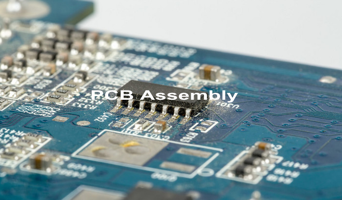
The assembly of a printed circuit board is the process of joining different electronic components to create a functional circuit. Many types of components are available, so there are many ways to combine them. Earlier, the electronic component manufacturers used to provide new types of components to electronic assemblers, but we are now experiencing a paradigm change. The electronics assemblers are now able to define the specifications for new components from the manufacturers. This encourages parts to be manufactured to conform to a current assembly process and allows the production of different assembly methods for which specific parts are necessary. The electronics assembly has, therefore, become a complex operation.
In the general context, the circuit board assembly is about putting a multitude of electrical parts and devices together to create a functioning, reliable appliances. This article deals with electronics assembly and its multiple aspects, such as electronic assembly manufacturing and electro-mechanical assembly.
————————————————————-
Request Electronic Contract Manufacturing Quote, Pls Send PCB File to Sales@raypcb.com Now
————————————————————-
Technologies Involved in Printed Circuit Board Assembly
Electronic assembly art demands that a variety of printed circuit board production techniques are available to assemble electronic parts. The technologies commonly used for electronic assembly are through-hole, surface mount, and a hybrid of these two techniques.
Through-hole Technology
Through-hole technology uses holes in the printed circuit boards (PCBs) to secure components with wire leads. Normally, one or both sides of a PCB have a conductive track that connects different components to form a circuit. Similarly, there are conductive tracks on the inner layers of the PCB if the board is multilayer. Wire leads of the electronic components are inserted through holes; around the holes, there are conductive pads which are used to join components with tracks using soldering. The fact that the component leads are installed on the board through holes is responsible for the term through-hole technology.
Surface Mount Technology
In surface-mount technology, the assembly principle is the same as through-hole technology: Mounting and soldering discrete electronic components onto a PCB. However, where through-hole printed circuit components are mounted with their wire leads inserted through holes in the board, the surface mount principle is simply placing leadless components on the board’s surface prior to soldering.
Hybrid Techniques
Hybrid techniques involve using through-hole and surface mount in combination with various other methods. Today most PCBs include devices of multiple technologies. Likewise, there are film technologies that are used to create some passive components on PCBs. Two types of film technologies exist, one is thin-film, and the other is a thick film. In the thin film, passive components are assembled by vapor deposition and etching. In the thick film, the components are assemblies by printing, drying, and firing pastes.
Through-hole has limited applications for modern PCBs because the components based on this technology cannot be miniaturized after a specific limit. Surface-mounted assemblies can be made significantly complex. Advancements in soldering techniques have made surface mounting accessible. The key factor is the soldering process used, with Reflow processes being the most common. In Reflow soldering processes, the solder is applied first, in the form of solder paste.
————————————————————-
Request Electronic Contract Manufacturing Quote, Pls Send PCB File to Sales@raypcb.com Now
————————————————————-
Assembly of PCBs
A Printed circuit board (PCB) is made up of the following components:
- A foundation is a small insulating substance board supporting all the elements that make up a circuit.
- Conductive connection traces on one or both sides of the foundation that make up the interconnections between modules; they are generally made up of copper.
Components are attached to pads, which are the track areas explicitly marked for part attachment purposes, by soldering. Since tracks are not printed directly into the surface, the word printed is somewhat confusing. Instead, it applies to only one step in the construction phase of the whole PCB. It is possible to produce printed circuit boards in one of two important forms. Firstly, the conductive tracks can be applied to the substrate’s surface or the base material in an additive phase. Second, the entire surface is coated with a conductive substrate in a subtractive method.
Printed circuit boards have been around as an electronics assembly technique in one form or another for fifty years. They didn’t gain significant use until the 1960s, when transistor circuits became more popular. Valve circuits have always been built by the direct positioning and manual soldering of individual connecting leads between the required circuit parts. Among other things, electronics assembly using a printed circuit board means that:
- Circuits are repeatable. After a prototype has been finalized, all the following circuits will be exact copies, unlike the situation in the previous interconnection assembly method.
- The insertion of components may be automated.
- Soldering of components may be automated.
- The testing of the final product may be automated.
- Products may be manufactured in large quantities, more cheaply.
- Reliability increases.
In most circuits, transistors have been superseded by integrated circuits (ICs). Even more than transistors, integrated circuits require a method of circuit assembly. Even the simplest 8-pin dual-in-line (DIL) integrated circuit requires a printed circuit board for assembly into its complete circuit. Modern integrated circuits with many more external connections are now available, for example
First transistor-based printed circuit boards were quite simple. Transistors are discrete components, and so only a limited number will fit on to a printed circuit board. The number of individual copper tracks on a board was always small. Positions of component lands were not critical, as connecting leads could themselves be adjusted to suit.
The majority of development work in electronics assembly techniques is now directed towards printed circuit boards in one form or another. The PCB and PCB Electronic Assembly is of most interest to the electronics manufacturing engineer. The greater number of connections per component means that a greater number of tracks per unit area results. The constant requirement for greater and greater packaging density results in integrated circuits with more and more connections.
Types of PCBs
Many forms of circuit boards are available. At least one new type of board must follow it each time a new part is created. The PCB categories are a little overlapping, and they are also pretty random so that each individual board will fall into many groups.
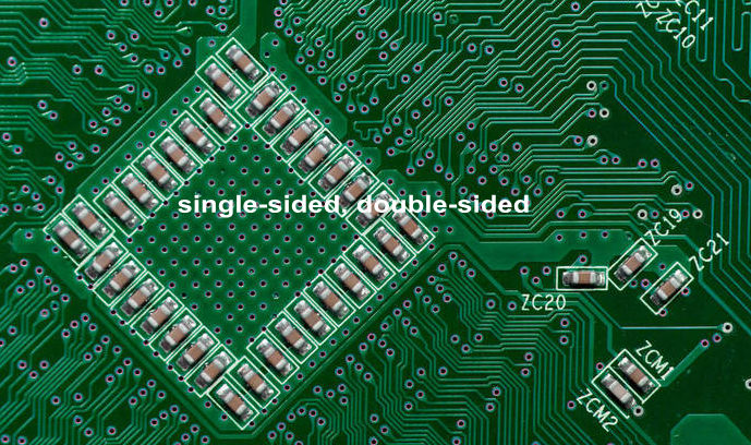
Single-Sided PCBs
A single-sided PCB contains conductive tracks on only one side of the base material. Usually, but not always, the components are mounted only on the other side. Holes are usually drilled or punched at pads’ locations; these pads are used for inserting component leads before the process of soldering.
Double-Sided PCBs
On all sides of the base material, double-sided PCBs have tracks. This helps the density of components to increase dramatically without reducing the trace widths. Typically, contacts between the traces on opposite sides ought to be made. The standard is to, in any plating procedure, coat the walls of holes with metal. Such plated-through holes (PTHs), which are for the specific purpose of track connection, are known as vias.
————————————————————-
Request Electronic Contract Manufacturing Quote, Pls Send PCB File to Sales@raypcb.com Now
————————————————————-
Multilayered PCBs
There are many layers of tracks on multilayer boards, two of which (as double-sided PCBs) are on the panel’s outer surfaces. The rest are internal to the base material, laminated together with insulating layers to provide electrical insulation, with PTH vias to provide the electrical connections needed. Holes used purely for connection purposes are known as through vias, while vias that do not pass entirely through the board are called buried vias or blind vias.
Miscellaneous Types of PCBs
After these three categories of the printed circuit board, all the following types can be seen to be derivatives.
Multi-wired printed circuit boards are, effectively, multilayer boards, with one essential difference. Layers are added externally and are not internal laminations. The wire is laid on to the substrate using a computer-controlled stylus, building up the remainder of the circuit one connection at a time. The insulation on each wire allows multiple crossovers, which means that too complex circuits can be laid in one extra layer.
Molded PCBs feature an injection-molded thermoplastic as the board base material. The base is plated to form the circuit, and other features can be incorporated. They are also called 3-D molded circuit boards.
Flexible printed circuit boards are produced using the methods already listed (with the current exception of multi-wire), using a flexible, rather than rigid, base material. All features, such as PTH vias and multilayer construction, are available. Flexi-rigid printed circuit boards combine flexible circuits with rigid boards so that the rigid board is said to have a flexible tail. If two such rigid boards are joined using a flexible circuit, they may be folded to give a multiple-tiered arrangement.
Although included here, hybrid and surface mounted assemblies are not different categories of printed circuit boards. They are; instead, variations of the categories already listed. However, the difference between component mounting systems in hybrid and surface mounted assemblies compared with those of ordinary printed circuit boards should be stressed. Hybrid assemblies are combinations of thick- or thin-film passive components, on to which discrete leaded or leadless passive and semiconductive components are mounted.
Surface-mounted assemblies, on the other hand, are simply a development of printed circuit and hybrid processes, where leadless components are used. In practice, increasingly, standard printed circuit board assemblies with leaded components may have a number of leadless components surface mounted, too. Where standard printed circuit boards rely on the insertion of components, the components’ leads go through holes in the board before soldering. Some hybrid and all surface mounted assemblies rely on components being merely placed on the board before soldering. Holes are not used to attaching mounted surface components – if holes do exist, they are plated-through holes and used as vias, which is interconnections between track layers only. This elimination of through-holes effectively means two things:
First, Components are held by small butt or lap soldered joints instead of large through-hole connections. This means that manufacturers have to be aware of potential stresses which can break these small joints. Secondly, the surface-mounted components enable parts to be manufactured with larger numbers of leads, and they can be placed more closely. This, in turn, means that packing densities are automatically increased. However, due to increased packing densities, problems can arise due to the heat generated within such small spaces. So boards which eliminate or at least reduce the effects of heat may have to be used.
PCB Assembly Manufacturing
This section defines the main processes which make up the techniques. Many of these processes are used in more than one technique, which creates a problem in clearly describing the techniques. It is assumed that the reader is familiar with any preceding process. Suppose a process is found, which is not described anywhere in the text describing a technique that is, hopefully, because it has been described previously. Printed circuit boards can be of three main types: single-sided, double-sided, and multilayered. This method takes into account the manufacturing processes involved in producing the conductive track.
There are two main manufacturing techniques. The first starts with the copper-clad base material and uses an etchant to dissolve away copper, which is not needed. This is called subtractive manufacturing. Purely subtractive techniques are often classed as conventional techniques. Printing a pattern on the copper surface which corresponds to the required track. Some form of etch resist chemical is used here to protect the track during the following step. Etching away the unwanted areas of copper from the board surface, leaving behind the wanted track.
Additive manufacture is the process of adding copper to a base laminate to make it laminate. The process is time-consuming and, often, complicated. Adds copper to laminate without copper, then adds the track where required. Most printed circuit boards are made using mixtures of additive and subtractive processes. Usually, the copper-clad base material is the starting point. The thickness of the copper laminated layer is much less than in subtractive manufacturing.
Testing PCB Assembly
Boundary-scan, in-circuit test (ICT), and flying probe are the most common test methods used in electronic PCB assembly. Plan the PCB assembly in a manner that is convenient for efficient development as well as research. When deciding which choice better fits your requirements, the product’s complexity, batch sizes, and budget would all be considerations. You can determine whether the development method integrates additional “power-up” or “working” checks.
Comments are closed