6 layer PCB fabrication is an essential process in the manufacturing of complex electronic devices. With the increasing demand for smaller and more powerful electronic devices, the need for high-density circuit boards has become more critical than ever before. The 6 layer PCB fabrication process involves the use of advanced techniques and materials to create a circuit board with six layers of copper traces and insulating layers, providing greater flexibility in designing complex circuits.
The process of 6 layer PCB fabrication begins with the design of the circuit board using computer-aided design (CAD) software. The design is then transferred to the fabrication plant, where the circuit board is manufactured using a combination of chemical and mechanical processes. The process involves the use of specialized equipment and materials, including copper-clad laminates, photoresist, etchants, and plating solutions. The result is a highly reliable and durable circuit board that can withstand the rigors of use in a wide range of electronic devices.
What is 6 Layer PCB Fabrication?
In the field of electronics, PCB or Printed Circuit Board is a crucial component that connects and powers various electrical components. It is a board made up of non-conductive material, usually fiberglass or plastic, with conductive pathways etched onto its surface. The number of layers in a PCB determines the complexity of the circuit, and the more layers there are, the more intricate the design can be.
6 Layer PCB Fabrication is the process of creating a printed circuit board with six layers of conductive pathways. This technique allows for a more complex circuit design, as well as the ability to incorporate more components into a smaller space.
The process of 6 Layer PCB Fabrication involves several steps, including designing the circuit, creating the layers, and assembling the board. The design of the circuit is typically done using specialized software, which allows for precise placement of components and pathways. Once the design is complete, the layers are created using a process called etching, where a chemical solution is used to remove the unwanted portions of the metal layer.
During the assembly process, the layers are stacked on top of each other and bonded together using heat and pressure. Once the layers are bonded, the holes are drilled, and the components are inserted and soldered into place.
In conclusion, 6 Layer PCB Fabrication is a process that allows for the creation of complex circuit designs with a higher density of components. The process involves several steps, including designing the circuit, creating the layers, and assembling the board. With the increasing demand for smaller and more powerful electronic devices, 6 Layer PCB Fabrication has become an essential technique in the electronics industry.
Advantages of 6 Layer PCB Fabrication
Increased Functionality
One of the main advantages of 6 layer PCB fabrication is the increased functionality it provides. With more layers, designers can add more components and connections, allowing for more complex circuits to be created. This is especially useful in applications where space is limited, as it allows for more functionality to be packed into a smaller area.
Higher Density
Another benefit of 6 layer PCB fabrication is the higher density it allows for. By adding more layers, designers can create more connections and components in a smaller area, allowing for higher density designs. This is particularly useful in applications where space is at a premium, such as in mobile devices or wearables.
Improved Signal Integrity
6 layer PCB fabrication can also improve signal integrity. By adding more layers, designers can create dedicated power and ground planes, which can help reduce noise and interference in the circuit. This can lead to better performance and reliability, especially in high-speed or high-frequency applications.
Overall, 6 layer PCB fabrication offers a range of benefits, including increased functionality, higher density, and improved signal integrity. These advantages make it a popular choice for a wide range of applications, from consumer electronics to industrial equipment.
Design Considerations for 6 Layer PCBs
Layer Stackup
When designing a 6 layer PCB, it is important to carefully consider the layer stackup. The layer stackup refers to the arrangement of the layers within the PCB, and it can have a significant impact on the performance of the board. Some important factors to consider when designing the layer stackup include the following:
- Signal integrity: The layer stackup should be designed in such a way as to minimize crosstalk and other signal integrity issues.
- Power and ground planes: It is important to include dedicated power and ground planes in the layer stackup to ensure proper power distribution and grounding.
- Thermal management: The layer stackup can also impact the thermal performance of the board, so it is important to consider thermal management when designing the stackup.
Impedance Control
Another important consideration when designing a 6 layer PCB is impedance control. Impedance is a measure of the opposition to the flow of electrical current in a circuit, and it is critical for ensuring proper signal transmission. Some important factors to consider when designing for impedance control include the following:
- Trace width and spacing: The width and spacing of traces can impact the impedance of the circuit, so it is important to carefully consider these factors when designing the board.
- Dielectric constant: The dielectric constant of the PCB material can also impact the impedance of the circuit, so it is important to choose a material with a consistent dielectric constant.
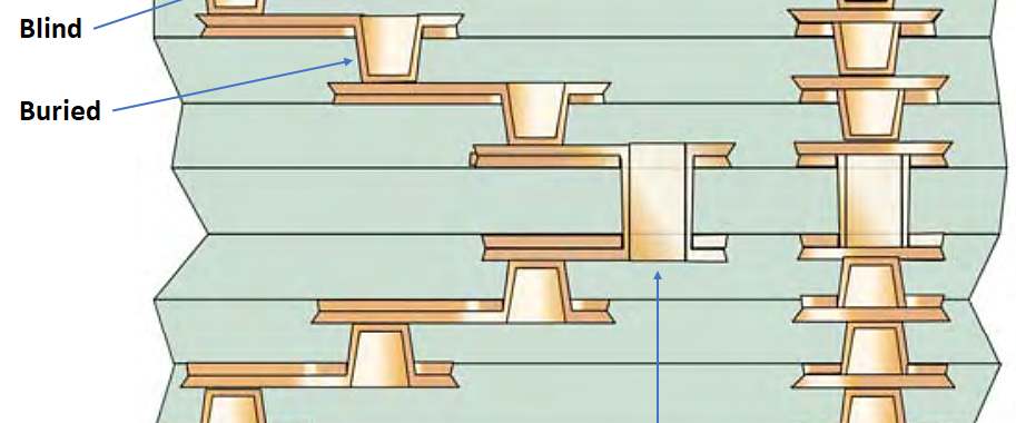
Via Types
Finally, when designing a 6 layer PCB, it is important to consider the types of vias that will be used. Vias are small holes drilled through the PCB that allow for electrical connections between different layers. Some important factors to consider when choosing via types include the following:
- Size and shape: The size and shape of the via can impact the electrical performance of the board, so it is important to choose a via size and shape that is appropriate for the application.
- Plating: The plating of the via can also impact the electrical performance of the board, so it is important to choose a plating material that is appropriate for the application.
In conclusion, when designing a 6 layer PCB, it is important to carefully consider the layer stackup, impedance control, and via types. By paying close attention to these factors, designers can ensure that their boards will perform optimally and meet the requirements of their application.
6 Layer PCB Fabrication Process
Preparation
Before beginning the 6 layer PCB fabrication process, it is important to prepare the necessary materials and equipment. This includes the PCB design file, copper-clad board, etching solution, solder mask, and silkscreen ink. The design file is typically created using CAD software and contains the layout and connections of the PCB.
Drilling
After the copper-clad board has been prepared, the next step is to drill the necessary holes for components and connections. This is done using a CNC drilling machine that accurately drills the holes according to the design file. It is important to ensure the drill bits are sharp and the board is held securely during the drilling process.
Plating
Once the holes have been drilled, the board is plated with a thin layer of copper to create the necessary connections between the layers. This is done using an electroplating process that deposits a layer of copper onto the board. The thickness of the copper layer can vary depending on the design requirements.
Etching
The next step is to etch away the excess copper from the board to reveal the desired connections and traces. This is done using an etching solution that dissolves the unwanted copper. It is important to ensure the etching solution is properly mixed and the board is agitated to ensure even etching.
Solder Masking
After the etching process, a solder mask is applied to the board to protect the copper traces and connections. The solder mask is typically a green or red layer that is applied using a silk screening process. It is important to ensure the solder mask is properly aligned and covers all necessary areas.
Silkscreen Printing
Finally, a silkscreen layer is applied to the board to label the components and connections. This is done using a silk screening process that applies the desired ink onto the board. It is important to ensure the silkscreen layer is properly aligned and legible.
Overall, the 6 layer PCB fabrication process involves several steps that require precision and attention to detail. By following these steps carefully, it is possible to create a high-quality PCB that meets the design requirements.
Quality Control in 6 Layer PCB Fabrication
In the process of 6 layer PCB fabrication, quality control is essential to ensure that the final product meets the required specifications. Quality control procedures involve visual inspection, electrical testing, and X-ray inspection.
Visual Inspection
Visual inspection is the first step in quality control. It involves checking the PCB for any defects that can be seen with the naked eye. The inspection includes checking for scratches, cracks, and other physical damage. It also involves checking for any missing or misplaced components.
Electrical Testing
After visual inspection, the PCB undergoes electrical testing. Electrical testing involves checking the PCB for any shorts or opens in the circuit. It also includes checking the resistance and capacitance of the components. Electrical testing ensures that the PCB functions correctly and meets the required specifications.
X-ray Inspection
In addition to visual inspection and electrical testing, X-ray inspection is also performed to check for any hidden defects. X-ray inspection involves using high-energy X-rays to penetrate the PCB and create an image of the internal structure. This allows for the detection of any hidden defects, such as voids or cracks in the solder joints.
In conclusion, quality control is an essential part of 6 layer PCB fabrication. The process involves visual inspection, electrical testing, and X-ray inspection to ensure that the final product meets the required specifications. By following these procedures, manufacturers can produce high-quality PCBs that meet the needs of their customers.
Applications of 6 Layer PCBs
Consumer Electronics
The use of 6 layer PCBs in consumer electronics has increased significantly in recent years. These PCBs are used in a wide range of products, including smartphones, tablets, laptops, and gaming consoles. The additional layers provide more space for routing traces and power planes, allowing for more complex designs and higher performance.
6 layer PCBs are also used in high-speed digital applications, such as HDMI and USB interfaces, where signal integrity is critical. The additional layers help to reduce noise and crosstalk, resulting in higher signal quality and faster data transfer rates.

Medical Devices
Medical devices require high reliability and precision, making 6 layer PCBs an ideal choice for these applications. These PCBs are used in a variety of medical devices, including pacemakers, defibrillators, and imaging equipment.
The additional layers allow for more complex designs, such as impedance-controlled traces and high-density interconnects, which are essential for these types of devices. Moreover, the use of 6 layer PCBs ensures that medical devices can operate safely and accurately in critical situations.
Aerospace and Defense
6 layer PCBs are widely used in aerospace and defense applications due to their high reliability and durability. These PCBs are used in avionics, radar systems, and other critical components.
The additional layers provide more space for routing traces and power planes, allowing for more complex designs and higher performance. Moreover, the use of specialized materials and manufacturing processes ensures that these PCBs can withstand extreme temperatures, shock, and vibration.
In conclusion, 6 layer PCBs offer a wide range of applications in various industries. From consumer electronics to medical devices and aerospace and defense, these PCBs provide high performance, reliability, and durability.
Comments are closed