Printed circuit boards (PCBs) have revolutionized the world of electronics by providing a compact, efficient, and reliable means of connecting electronic components. PCBs are used in a wide range of electronic devices, from smartphones and computers to medical equipment and aerospace technology. They are a fundamental part of modern electronics and have played a crucial role in advancing the field.
A PCB is a thin board made of insulating material, such as fiberglass or plastic, with conductive pathways etched onto its surface. These pathways, also known as traces, connect the various electronic components on the board, such as resistors, capacitors, and integrated circuits. The use of PCBs has many advantages over traditional wiring methods, including reduced size and weight, increased reliability, and improved performance. PCBs also allow for automated assembly, making the production process more efficient and cost-effective.
In this article, we will explore the world of PCBs and their role in modern electronics. We will look at the history of PCBs, their design and manufacturing process, and their applications in various industries. We will also discuss the latest developments in PCB technology and their potential impact on the future of electronics.
What is a PCB?
History
A printed circuit board (PCB) is a board made of insulating material on which conductive pathways are etched or printed. The concept of a PCB dates back to the early 20th century when Charles Ducas patented a method of electroplating circuit patterns on a non-conductive substrate. The first PCB was developed by Paul Eisler in 1936 for a radio set. Since then, PCBs have become integral parts of the electronics industry.
Functionality
PCBs provide a mechanical support and electrical connection for electronic components. They are used in a wide range of electronic devices, including computers, smartphones, medical equipment, and automotive systems. The conductive pathways on a PCB are usually made of copper, which is an excellent conductor of electricity. The insulating material, also known as substrate, is typically made of fiberglass, plastic, or ceramic.
Types of PCBs
There are several types of PCBs, each with its unique characteristics and applications. Some of the most common types include:
- Single-sided PCBs: These have conductive pathways on one side of the substrate.
- Double-sided PCBs: These have conductive pathways on both sides of the substrate.
- Multi-layer PCBs: These have multiple layers of conductive pathways separated by insulating material.
- Flexible PCBs: These are made of flexible materials, such as plastic or polyimide, and can be bent or twisted without breaking.
- Rigid-flex PCBs: These combine the features of rigid and flexible PCBs to provide a unique combination of flexibility and durability.
In conclusion, PCBs are an essential component of modern electronics. They provide a reliable and efficient way of connecting electronic components while reducing the size and weight of electronic devices.
Electronic Components and PCBs
Basic Electronic Components
Electronic components are the building blocks of electronic circuits. They are used to control the flow of electricity in a circuit. Some of the basic electronic components include resistors, capacitors, diodes, transistors, and integrated circuits (ICs).
- Resistors: These are used to resist the flow of current in a circuit. They come in different values and are used to regulate the voltage and current in a circuit.
- Capacitors: These are used to store electrical energy and release it when needed. They are used in filters, oscillators, and timing circuits.
- Diodes: These are used to allow current to flow in only one direction. They are used in rectifiers, voltage regulators, and signal detectors.
- Transistors: These are used to amplify or switch electronic signals. They are used in amplifiers, oscillators, and switching circuits.
- Integrated Circuits (ICs): These are complex electronic components that contain many transistors, resistors, and capacitors on a single chip. They are used in computers, cell phones, and other electronic devices.
PCB Design and Layout
Printed Circuit Boards (PCBs) are used to connect electronic components together in a circuit. They are made of a non-conductive material with conductive traces that connect the components together. PCBs are designed using computer-aided design (CAD) software and are manufactured using a chemical etching process.
- CAD Design: The design process involves creating a schematic diagram of the circuit and then laying out the components on the PCB. The CAD software allows designers to test the circuit and optimize the layout before manufacturing.
- Manufacturing: The manufacturing process involves printing the circuit design onto a copper-clad board and then etching away the unwanted copper using chemicals. The remaining copper forms the conductive traces that connect the components together.
- Testing: Once the PCB is manufactured, it is tested to ensure that it works correctly. Any defects are identified and corrected before the PCB is used in a circuit.
Soldering and Assembly
Once the PCB is manufactured and tested, the electronic components are soldered onto the PCB. Soldering is the process of melting a metal alloy to join two metal surfaces together. The solder creates a permanent bond between the component and the PCB.
- Surface Mount Technology (SMT): This is a method of soldering electronic components onto a PCB using automated machines. SMT components are smaller and more compact than through-hole components, making them ideal for small electronic devices.
- Through-Hole Technology (THT): This is a method of soldering electronic components onto a PCB using a manual process. THT components are larger and more robust than SMT components, making them ideal for larger electronic devices.
In conclusion, understanding basic electronic components, PCB design and layout, and soldering and assembly are essential skills for anyone working with electronics. By mastering these skills, you can design and build electronic circuits that are reliable and functional.
PCB Manufacturing Process
PCB or Printed Circuit Board is a crucial component in electronic devices. It provides a sturdy base for electronic components to be mounted on and connected to each other. The manufacturing process of PCB involves several steps that require precision and accuracy to ensure the final product is of high quality. Here is an overview of the PCB manufacturing process.
Design
The first step in PCB manufacturing is designing the circuit board. This involves using a computer-aided design (CAD) software to create a digital representation of the circuit board. The design includes the placement of electronic components, the routing of traces, and the creation of drill holes. The design file is then sent to the manufacturer for printing.
Printing and Etching
Once the design is finalized, it is printed onto a copper-clad board using a special printer. The printer prints the design onto a transparent film, which is then used to transfer the design onto the copper-clad board. The board is then etched to remove the copper that is not part of the circuit design. This leaves behind the copper traces that connect the electronic components.
Drilling and Plating
After the etching process, the board is drilled to create holes for the electronic components to be mounted on. The holes are then plated with a thin layer of copper to ensure a strong connection between the component and the trace. The plating also helps to prevent oxidation of the copper.
Testing and Inspection
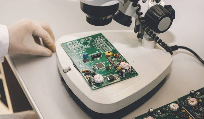
The final step in the PCB manufacturing process is testing and inspection. The board is tested to ensure that all the connections are correct and that there are no faults in the design. The board is also inspected for any defects or imperfections that may affect its performance.
In conclusion, the PCB manufacturing process involves several steps that require precision and accuracy to ensure the final product is of high quality. From design to testing, each step plays a crucial role in ensuring that the circuit board is functional and reliable.
Advancements in PCB Technology
Flexible PCBs
Flexible PCBs, also known as flex circuits, have gained popularity in recent years due to their ability to conform to different shapes and sizes. These PCBs can be bent, twisted, and folded, making them ideal for use in wearable devices, medical equipment, and automotive applications. Flexible PCBs are made using a combination of polyimide films and copper traces, which can be designed to fit specific shapes and sizes.
High-Density Interconnect PCBs
High-Density Interconnect (HDI) PCBs are designed to have a high density of components and connections on a small surface area. These PCBs are commonly used in mobile devices, such as smartphones and tablets, where space is at a premium. HDI PCBs use advanced manufacturing techniques, such as microvias and blind vias, to create a higher density of connections on the board.

3D Printed PCBs
3D printing has revolutionized the way PCBs are manufactured. With 3D printing, PCBs can be created quickly and easily, without the need for expensive tooling or equipment. 3D printed PCBs are ideal for prototyping and small production runs, as they can be manufactured in a matter of hours. They can also be designed to fit specific shapes and sizes, making them ideal for use in custom electronics.
In conclusion, advancements in PCB technology have led to the development of flexible PCBs, high-density interconnect PCBs, and 3D printed PCBs. These technologies have opened up new possibilities for the design and manufacture of electronic products, making them more efficient, compact, and customizable.
Applications of PCBs
PCBs have become an essential component in the modern electronic industry. PCBs are used in various applications, including consumer electronics, medical devices, aerospace, and defense.
Consumer Electronics
PCBs are widely used in consumer electronics, such as smartphones, laptops, and televisions. PCBs are used to connect and control the various components of electronic devices, such as microprocessors, memory chips, and sensors. PCBs also help reduce the size of electronic devices, making them more compact and portable.
Medical Devices
PCBs are also used in medical devices, such as pacemakers, defibrillators, and imaging equipment. PCBs are used to control and monitor the various functions of medical devices, ensuring that they operate correctly and safely. PCBs also help medical devices operate with high precision and accuracy, making them suitable for use in critical medical applications.
Aerospace and Defense
PCBs are used in aerospace and defense applications, such as satellites, missiles, and aircraft. PCBs are used to control and monitor the various functions of aerospace and defense equipment, ensuring that they operate correctly and safely. PCBs also help aerospace and defense equipment operate in harsh environments, such as extreme temperatures and high altitudes.
In conclusion, PCBs are an essential component in the modern electronic industry. PCBs are used in various applications, including consumer electronics, medical devices, aerospace, and defense. PCBs help reduce the size of electronic devices, ensure that medical devices operate safely and accurately, and help aerospace and defense equipment operate in harsh environments.
Comments are closed