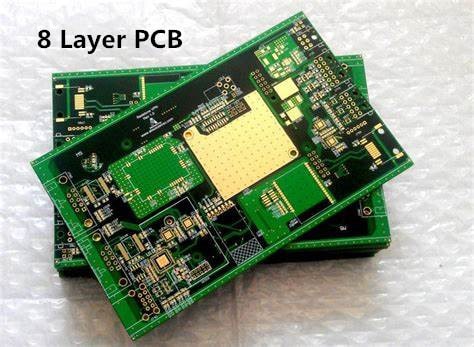
The 8 layer PCB has seen a tremendous rise in the use cases in recent times. It must be mentioned that the application of the 8 layer PCB stackup is broadening as the days go by because the circuit board can be used for many things.
In this article, we aim to help you understand the meaning of the 8 layer PCB. You will also learn about the prototyping, the guidelines, and the factors that will help you get the best designer.
What Is an 8 Layer PCB?
The first thing we want you to understand is the meaning of the 8 layer PCB. When you understand all there is to this circuit board, it will be easier for you to comprehend how it functions.
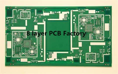
The 8 layer PCB stackup is a type of Printed Circuit Board (PCB) that has the layers firmly stacked. The stacking goes on to create a formidable dependable and predefined mutual connection among all the layers on the board.
It must be noted that the procedure of designing and producing the 8 layer PCB stackup isn’t as easy as mounting the components. Instead, a complex manufacturing procedure is always used to design the circuit board.
8 Layer PCB Prototype
The prototype of the 8 layer PCB isn’t something that takes more time than required. Instead, the designer or PCB manufacturer needs to have an eye for details to make the design work out as planned.
Because of the complexity of the structure, it may take some time before the design of the 8 layer PCB will be completed.
Having said that, here are some of the steps that are required when creating or designing the prototype of the 8 layer PCB:
Impedance Control
Isolation and Impedance Control is needed on the traces because of the roles that play in the overall success of the 8 layer PCB design.
In that case, the use of the Isolation and Impedance Control is required for those analog signals that require RF.
Prevention of Noise Decoupling
Noise decoupling is an important aspect that must be considered when designing an 8 layer PCB.
It is important to prevent that and the best way is to create a digital ground plane. It is in this ground plane that the multiple power and ground planes will be designed and deployed via the 8 layer PCB stackup.
Layer Matching
The layers in the 8 layer PCB must be matched. The ideal way of going about that is by creating more layers that will be used in aiding routing signals.
Signal Shielding
Signals ought to be shielded from one another to prevent loss of signal and infractions.
That informs the reason why the 8 layer PCB is the best circuit board in that regard. It provides more planes, which, in turn, will be used for shielding signals from the other signals on the adjacent layers.
Guidelines to an 8 Layer PCB Stackup
There are some guidelines and prerequisites to be met before the 8 layer PCB can be deployed.
Here are the different guidelines that aid the successful use of this type of Printed Circuit Board (PCB):
Improving EMC Performance
The first guideline of the 8 layer PCB is that the performance of the EMC will be improved tremendously.
Sometimes, that improvement is tenable when additional planes are added to the circuit board.
More Routing Layers
The addition of more routing layers is the other aspect of the 8 layer PCB stackup. In this case, the 8 layer PCB is used to add more routing layers (usually two) so that the same will be used to enhance the performance of the EMC.
Configuration of an 8 Layer PCB Stackup
There has been some confusion over the configuration and outlook of the 8 layer PCB. When you understand that, it becomes a lot easier for you to find out how the circuit board looks like after it must have been designed.
Four Layers and Four Planes
The 8 layer PCB stackup doesn’t have eight (8) layers as many customers may have presumed. Instead, the circuit board consists of four planes and four layers.
Better EMI Control
Having better control over the EMI is another aspect of the 8 layer PCB configuration. The idea is to make it easier for the functions and operations of the circuit board to be well controlled.
Aside from that, the signal integrity of the design will be improved and increased when that is put into consideration.
The composition and configuration of the 8 layer PCB go on to create signal layers that are separated by the ground planes and the power planes. The role of those planes is to increase the strength of the signals by reducing the crosstalk between the signal layers.
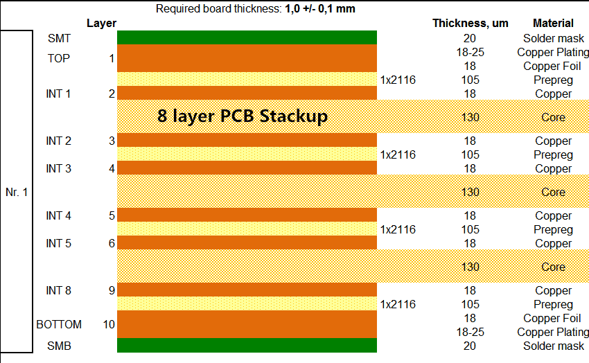
Below is how the 8 layer PCB tends to look like at the end of the design:
- Top layer
- Prepreg
- Ground plane
- Core
- Inner Layer 1
- Prepreg
- Power plane
- Core
- Ground plane
- Prepreg
- Inner Layer 2
- Core
- Power plane
- Prepreg
- Bottom layer
Best Practices for an 8 Layer PCB Stackup Design
There are some techniques and best practices that must be adhered to anytime you want to design the 8 layer PCB.
Here are some of those techniques and the roles they play:
1. The Direction of the Routing
The first technique is to master how to route the layer. More often than not, there may be some mix-up in routing the signal layers.
The ideal way of going about that is by using perpendicular routing to route the signal traces on the adjacent layers. Doing that ensures that the risks of crosstalk will be minimized.
For added effect, consider routing the signal layers differently on the subsequent layers. This is despite the separation of those layers by the ground and the power planes.
2. Buried or Blind Vias
More space can be created on the 8 layer PCB for routing only if the right machinery is in place. That machinery is to use the buried or blind vias.
However, not all 8 layer PCB manufacturers and designers have the tools to make this work. So, you want to confirm with the designer if the buried or blind vias option can be used in designing your 8 layer PCB stackup.
3. Return Path
The Return Path can make or mar the outcome of the 8 layer PCB design. So, it is pertinent that you understand how the Return Path is designed to work on the circuit board.
The rule of thumb is to ensure that the 8 layer PCB has a short Return Path. This does not only help to reduce the risks of interferences with the other components. It is also helpful in facilitating high-speed signals.
4. Ground Plane
As much as the ground plane helps to create the needed signals, it must be designed in the right way.
Ideally, the best way of designing the ground plane is to ensure that it isn’t split. A split ground plane can create impedance discontinuity on the 8 layer PCB stackup.
Aside from ensuring that the ground plane isn’t split, also check to see that the outer layer components have low impedance. That is especially considered when the impedance is connected to the inner ground planes via the vias.
The Cost Considerations for an 8 Layer PCB Stackup
Designing an 8 layer PCB costs money. It makes sense that you have an idea of the rough estimate of what it will cost you so you wouldn’t be disappointed when the costs exceed what you budgeted.
Below are some of the cost-affecting factors that contribute to the increase in the cost of designing the 8 layer PCB stackup:
Number of Layers
The first consideration is the number of layers that the Printed Circuit Board (PCB) has.
Contrary to the popular opinion that the 8 layer PCB has eight layers, it instead has four. The other four components are the four planes.
Size of the Board
The size of the board has to do with the components therein. The more components are packed into the board, the more the size increases.
The 8 layer PCB stackup board size increment can contribute to an increase in the cost of designing and manufacturing the circuit board.
The Size of the Holes
The size of the holes on the 8 layer PCB is another important factor that can influence the costs of the circuit board.
We will look at this from two perspectives. The first perspective dictates that the more holes are needed on the board, the higher the costs of design and production. The other perspective has to do with the use of super-thin holes that require more work before the board will be produced.
Type of Finish
Despite being designated a minimal factor, the type of finish used in the 8 layer PCB can increase the costs.
Of course, you have many options when it comes to this. You may want to use the type of finish that offers a longer shelf life or another that has a higher grade.
Here are some of the most popular types of finishes used on the 8 layer PCB stackup:
- ENEPIG: This type of finish is used because of the solderability, the contact-surface, and the AI Wire bondable feature.
- HASL
- IMM Ag
- OSP
- Elec Au
- LFHASL
- ENIG
- IMM Sn
Custom Specifications
More often than not, some customers will want the 8 layer PCB to have some specific configurations and specifications to make their design unique.
Of course, if this is to be considered, it means more expenses will be made, as the manufacturer has to take more time to work on the project.
Therefore, as you are coming up with the custom designs and specifications for the 8 layer PCB stackup, ensure you have some more money to spare.
Thickness
The thickness of the 8 layer PCB has to do with the materials used to enhance the sturdiness of the board. If you are considering this, have in mind that the thicker the circuit board gets, the more costs it will attract.
In the same regard, the type of materials used for the design can contribute to an increase or a decrease in the thickness of the board. If the materials aren’t too thick, you may spend less.
How to Find the Best 8 Layer PCB Stackup Designer
Finding and using the services of a good 8 layer PCB manufacturer is a matter of patience. You must be careful about how you go about that so you wouldn’t have to get the design that you didn’t expect.
Here are some of the factors and the things to look for when looking to hire an 8 layer PCB manufacturer:
1. One-to-One Service
You might want to use the same PCB designer for all your 8 layer PCB stackup needs. That way, you are confident that the design will be facilitated in real-time and at affordable costs too.
Besides, an 8 layer PCB manufacturer/designer that offers a one-stop service helps to source the materials and get all the specifications ready for immediate design, manufacture, and dispatch.
2. Professionalism
You wouldn’t want to use an 8 layer PCB manufacturer that doesn’t have the relevant experience and expertise.
Aside from the professional undertone, you must also consider the certifications the manufacturer has, as that will help you make an informed decision.
3. Order Capacity
Does the 8 layer PCB manufacturer have the capacity to deliver the project and on time?
You must also check to see if the manufacturer/designer can take the minimum quantity that you want to design and manufacture.
4. Turnaround Time
Can the 8 layer PCB manufacturer facilitate the design and manufacture of the circuit board in a few weeks?
If that’s not tenable, can the manufacturer be able to deliver the design in good condition at the time you need it?
Find out with the 8 layer PCB manufacturer you want to use if the turnaround time is feasible.
Final Words
Finding an 8 layer PCB manufacturer/designer for your next project/design wouldn’t be a herculean task after all.
The tips we shared will help you in making an informed decision on what to expect on the 8 layer PCB and how you can get the best designer/manufacturer for the job.
Comments are closed