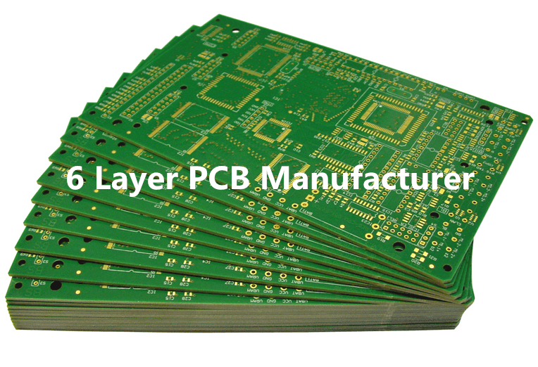
Printed Circuit Boards (PCBs) are growing in popularity because of the flexibility they offer to electronic appliances. So, when the 6 layer PCB is brought into focus, it means the use cases will be higher.
What Is a 6 Layer PCB
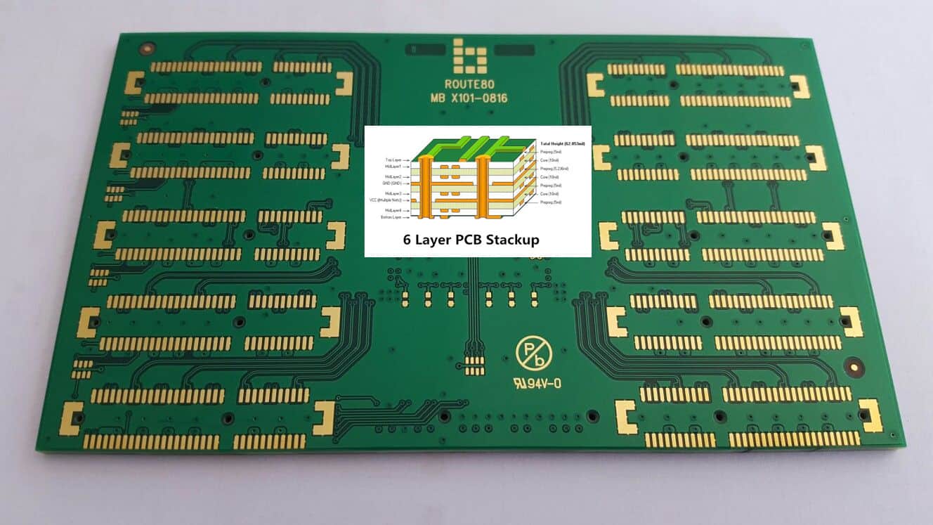
The 6 layer PCB stackup is the type of Printed Circuit Board (PCB) that uses 4 layers. This may seem surprising considering that the name implies 6 layers. However, that is not always the case because the 6 layer PCB has a variation to it.
By and large, the 6 layer PCB stackup is a circuit board that has 4 layers attached to the board while two additional layers are added between the planes.
Design of the 6 Layer PCB
It must be mentioned that there are some specific requirements to be met before the 6 layer PCB can be actualized.
The first consideration is the classic stackup that has to do with the four (4) routing layers. These layers are divided into:
- Two internal layers
- Two outer layers
The other two layers that make up the 6 layer PCB prototype are used between the internal planes. These are the use of one of the layers in the power and the other on the ground of the circuit board.
It should be noted that the overall impression of the 6 layer PCB is geared towards facilitating the viabilities of the circuit board. Ideally, the EMI will be drastically enhanced and improved when the 6 layer PCB is used. Some of the ways it is done are by:
- Delegating two surface layers that will be used for routing low-speed signals
- Offering two buried layers that help release high-speed signals
Variations in the 6 Layer PCB
As much as the 6 layer PCB has many potential benefits and use cases, there are also some cases where the actual design may not be tenable. Instead, there are two major variations to the use of the 6 layer PCB.
The first variation is that it that the circuit board’s route traces will be routed to the adjacent routing layers on a perpendicular basis. It is because of it that the 6 layer PCB tends to have minimal crosstalk and increased routing efficiency.
The other variation stems from the speed of the 6 layer PCB. If you are considering the high-speed designs, for instance, it means you will have to keep the ground and power planes on the adjacent layers. While that aids in decoupling, the additional ground planes may also be used for shielding the designs that may require low electromagnetic emissions.
Tips to Help You Choose a 6 Layer PCB Vendor
Are you ready to design your next 6 layer prototype? You will need a PCB manufacturer/vendor that has been in that field for many. The vendor also needs to have a mastery of the different concepts that will make the design great.
Finding a good 6 layer PCB manufacturer isn’t always an easy task. You will continually check through the hundreds of manufacturers, comparing their services against the other.
But, if you are ready to save the time and efforts to go through that long track, we are ready to help you.
We have come up with important features and considerations that you must always have in mind when you want to choose a 6 layer PCB manufacturer. Here are some of those tips:
1. Instant Quotation
Nobody has all the time in the world. You certainly don’t have that too. And even if you had some time to spare, you wouldn’t want to use it to beat around the bush.
The first thing you should be looking for is the availability of instant quotes. More often than not, the 6 layer PCB manufacturer has a section on the website where you can enter the details of the design for a breakdown of the costs.
Here are some of the requirements and details you will be required to enter to get a quote:
- Quantity or the number of 6 layer PCB you want to be designed for you
- The thickness of the circuit board
- The number of layers you want. Because this is a 6 layer PCB, you should select 6 layers and not 4 layers.
- Dimensions of the circuit board (height x width)
2. The PCB Layout
The success of a 6 layer PCB design is partly because of the manufacturer’s expertise and mainly because of the layout of the board. If the circuit board wasn’t laid out the way it should, it wouldn’t be long before issues will start coming up.
It is for that reason you must consider the design of the 6 layer PCB layout, as it plays an important role in the success of the design.
To inspire you, here are some of the important aspects of the PCB layout design that you must focus on at all times:
DFM Team
This has a lot to do with the manufacturer. If the manufacturer can’t deliver on the job, don’t use its services.
But, how will you know a manufacturer that can deliver the best 6 layer PCB layout design? It is simple! Check to see if the manufacturer has a DFM team, which is the team that will manufacture the design you want.
Types of Vias
While vias play an important role in the design of a 6 layer PCB, too much of it may not be ideal.
Sometimes, the manufacturer may want to try many things at different times by using many types of vias in your 6 layer PCB.
That shouldn’t be the case because the diversification and overt use of the vias may make the design awkward. Instead, aim to use the services of a 6 layer PCB manufacturer that uses minimum vias for the 6 layer PCB design.
PCB Stack-Up
PCB Stack-Up implies the trade-off or the advantage between the layer count and the fabrication process.
Always aim to have a PCB Stack-Up that aligns with the cost targets, desired reliability, and yield of the circuit board.
3. Thermal Relief
There is no denying that there may be a need to get some thermal relief if the circuit board becomes too hot. Of course, you may not always actualize that if you hadn’t figured it out from the onset.
It must be mentioned that issues that have to do with the terminals/thermal points of the 6 layer PCB may cause great damages.
There are many ways to curtail excessive hotness on the 6 layer PCB. Here are some of them:
Sufficient Spaces
Is it possible to have more spaces in a Printed Circuit Board (PCB) considering that the boards are now getting smaller?
Yes, it may be possible if the 6 layer PCB manufacturer has expertise in that regard. What is required is to create more and sufficient spaces around those areas that tend to get hotter with time.
Have in mind that the reason for the increased hotness is because the current passing through the traces gets higher with time.
Besides, having more space on the circuit board is a must because the more space is available, the more the heat will have enough area to cool off.
4. Single Point of Contact
It is time you stopped searching for different hands to help you manufacture your 6 layer PCB. Instead, aim to have a single point of contact or a one-stop-shop whereby the manufacturer will handle the design from the start to the finish.
Here are some of the reasons why you should use only one 6 layer PCB manufacturer:
Eliminates Communication Barriers
The first reason for selecting one 6 layer PCB manufacturer is that it helps to eliminate communication barriers.
If you were using different manufacturers, the potentialities of confusion tend to be many. That is because you will keep trying to get information from different angles and using the same to inspire the other party.
Fewer Modifications
Modifications are paramount when there must have been some errors in the course of the PCB design.
While it may not be entirely ruled out, it can be reduced when only one hand is working on the design. Also, if the 6 layer PCB manufacturer is handling the design and manufacturing, it becomes a lot easier to spot the errors on time.
Fixing those errors and making the needed modifications wouldn’t be a mirage, as everything is done in-house.
5. Component Sourcing
Most times, customers believe that a 6 layer PCB manufacturer offering one-shop services should also handle the component sourcing. While that is usually the case, you needn’t leave it all to the manufacturer.
Rather, consider taking the time to check how the component is sourced, as you may need to do it yourself sometime. At the same time, ensure that the manufacturer or designer of your 6 layer PCB is using the right type of component on the circuit board.
6. Power and Signal Integrity
If the integrity of the signal and the power is not optimum, there is a likelihood that the design of the 6 layer PCB may not come off as expected.
So, what can be done about it? It is to bolster the power and signal integrity. Here are ways to go about it:
Check the Aspects
The first step is for the engineer designing the 6 layer PCB to check the aspects of the circuit board.
Here are some of the aspects that ought to be checked:
- Terminations
- The rise and fall of the signal times
- Characteristic impedances
- The drivers’ slew rates
- Drive strength
- Track lengths
DC and AC Performance
The integrity of the power is mostly buoyed by the performance of DC and AC. You want to check to see if the overall performance of the DC and AC in the power distribution network is optimum.
Integrity Simulations
There may be no better time to check the integrity of the power and signal than before the commencement of the design.
The ideal way to do that is by performing the signal integrity simulations during the pre and the post layout of the 6 layer PCB.
7. Component Placement
How the 6 layer PCB manufacturer places the components is another point of concern.
We understand that different PCB manufacturers have different approaches to mounting the components on the circuit board.
However, the standard placement model mustn’t be deviated from because that may alter the outcome of the design.
In light of that, here is the ideal way of placing and mounting the components of the 6 layer PCB:
- The connectors should come first
- The power circuits should follow
- The precision circuits will be mounted followed by the precision circuits
- After all those aforementioned components have been mounted, the other elements and components will follow suit.
8. Cost
What is your budget for the 6 layer PCB design? More often than not, the budget you have is only a placeholder because the actual costs may be higher than what you set aside.
Despite that, you will want to select and use the services of a 6 layer PCB manufacturer whose costs of the design and manufacturing is closer to what you budgeted.
9. Turnaround Time
How long will it take the manufacturer to design the 6 layer PCB, manufacture it, and send the same to you?
That is why you must consider the turnaround time, especially when you want to take delivery of the 6 layer PCB as soon as possible.
10. Mode of Delivery
How flexible and efficient is the delivery system of the 6 layer PCB manufacturer? Some of those manufacturers have an ongoing relationship with logistic companies like FedEx, which enables them to dispatch the circuit boards in time.
By and large, aim to choose a 6 layer PCB manufacturer that can deliver the circuit board within five (5) business days.
Conclusion
The 6 layer PCB brings more flexibility and applications to the areas you intend to use it.
Ensure that you are outsourcing the design and manufacturing of the circuit board to a PCB manufacturer that can deliver the best quality and at affordable costs too!
Comments are closed