Printed Circuit Boards (PCBs) are used by electronics companies to protect the electrical connections and components in their appliances. The beauty of it all is that the wiring is not revealed, thereby, making it less threatening.
In the global PCB industry, different designs have been used to design and manufacture Printed Circuit Boards (PCB). HDI is one of the variants and models of the Printed Circuit Board (PCB).
The aim of this content is to give you a complete guide on what the HDI PCB is all about. You will also learn about where to find a good HDI PCB manufacturer and other important information you will need.
What Is HDI PCB?
So, what is this HDI PCB that you have been hearing about? Is it a type of Printed Circuit Board (PCB) that works better than the traditional PCB?
Indeed, the HDI PCB has better functionalities and precision than what we have been having in the other PCBs.
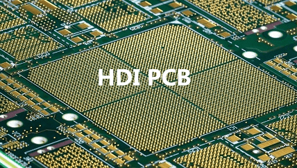
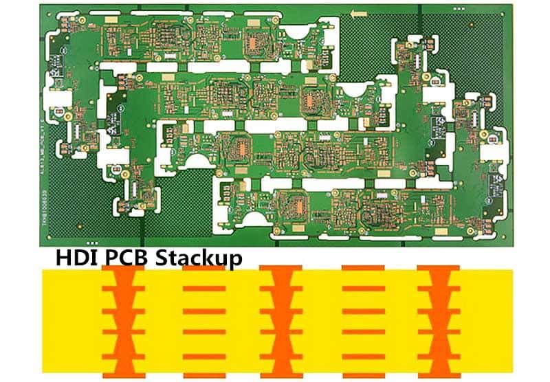
The HDI PCB is a type of circuit board that features better wiring than what the traditional Printed Circuit Boards (PCBs) have to offer. With the full name as High Density Interconnector (HDI), the HDI PCB aids in the reduction of the electrical equipment/component’s weight and size. It is also used for the enhancement of the electrical performance of the circuit board.
What Makes the HDI PCB Better Than the Traditional Circuit Boards?
You must understand the basics so you will have a better comprehension of the differences that exist between the HDI PCB and the conventional circuit boards.
The first difference is that the HDI PCB offers better precision and performance of the electrical signals. That is because of the high-level protection provided by Micropore Technology. The increased and higher density of the HDI PCB is another reason why the HDI PCB doesn’t have much interference to reduce the operations.
The second reason why the HDI PCB will continually beat the traditional circuit boards is because of the compact size. The compactness of its circuit board is accentuated by the drastic decrease of the aperture range. The decrease enables a further decrease in the pad size. Therefore, it becomes easier for multiple components to be added to the circuit board.
Finally, hiding the wiring is a matter of convenience when using the HDI PCB. That is because of the obvious role played by the Circuit Density that enables the hiding of the wires. When this is done, more advanced electronics can use the HDI PCB because of the higher appeal and small size.
Advantages of HDI PCB
It is now popular that the HDI PCB has better and advanced features than what we have been seeing on the traditional Printed Circuit Boards (PCBs). Since that is the case, it implies that the circuit board has some advantages that it has over the former.
Here are some of the features, properties, and advantages of the HDI PCB:
1. Less Heat Transfer
It is no secret that the presence and dominance of heat on a Printed Circuit Board (PCB) can be the singular reason why it may damage in a short while.
Something can be done about that. It is by reducing the presence of heat and transferring the same in time.
The HDI PCB does that excellently. The circuit board does a great job of facilitating the transfer of less heat. At the same time, the heat will be made to travel farther before its escape from the High Density Interconnector (HDI) circuit board.
2. Extended Battery Life
You must care for the batter life and longevity of the HDI PCB, as much as you are caring for the performance.
It must be mentioned that the High Density Interconnector has a higher and extended battery life because of the reduced power consumption.
3. Reliable Transmission
The reliability of transmission on the HDI PCB is because of the compact size that comes in handy when adding more components.
That is the reason why the addition and incorporation of the BGA and OFP packages wouldn’t be a tough task because the HDI circuit board can accommodate them because of their smaller sizes, and because of the more space on the circuit board.
4. Populated Sides
The sides of the HDI circuit board are populated. The reason is that it allows the PCB designer and manufacturer more space to add more components that will make the job successful.
5. Reducing the Weight of Products
The use of the HDI circuit board plays an excellent role in the reduction of the weights of products.
You will recall that the board has a compact size that makes it easier for it to fit into any type of product to be designed and manufactured. Also, it hides the wires very well so that wouldn’t be an obstruction during the coupling.
6. Many Applications
The areas and use cases of the HDI PCB is not limited. Instead, the circuit board can be used for many things and on many products.
Some of the use cases and the applications are:
- Medical devices
- Fourth Generation (4G) network communications
- Electronic aircraft parts
- Digital cameras
- Mobile phones
- Laptop computers and
- Touch-screen devices
7. Fast Turnaround Time
Customers are always looking for a PCB manufacturer that will design and manufacture their circuit boards in real-time. While the manufacturer or designer may offer a fast turnaround, the type of circuit board must also be considered.
The amazing thing about the HDI PCB is that it offers a fast turnaround time. This is for many reasons. The first reason is that there is no need to constantly relocate the components of the circuit board. The second is that the SMD components are easily placed on the circuit board.
The last but not the least is that the HDI PCB requires sophisticated technology. The sophistication of the technology is bolstered by the laser technology that aids in the facilitation of the design.
Features of the HDI PCB
How do you know or identify an HDI circuit board? There are many ways to spot a good one.
Here are some of the features you must look for when looking to design an HDI circuit board:
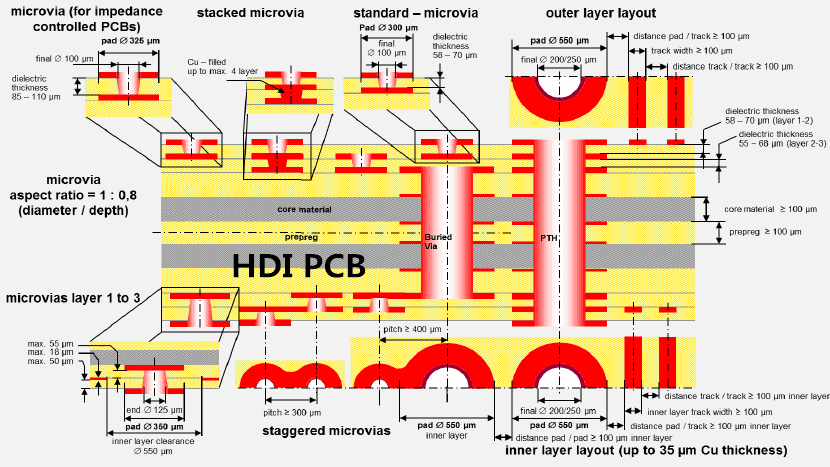
Blind Vias
The first feature or property of the HDI PCB is the blind vias. In addition to that, the blind vias often tag along with the buried vias and the micro vias. The trio often has a diameter of 0.0006mm or less.
Minimized Pad Size
The size of the pad is also minimized because of the significance of the line width of about 4.0 mil and the aperture within the range of 3.0 to 6.0 mil.
The other features of the HDI circuit board include but are not limited to:
- Higher pad densities
- Incorporation/addition of finer spaces and lines
- Higher connection
How to Evaluate an HDI PCB Manufacturer
It is time to design your next HDI PCB. How do you know the designer and manufacturer that will go a great job?
This is not something that will be determined on the surface level or by guessing. It has more to do with the knowledge of the features to look for and where to look for them.
We are committed to ensuring that your next HDI circuit is successful. To that end, here are some of our tips on how you can find a good HDI PCB manufacturer to handle the job for you.
1. Smooth Transition from Prototype to Production
The work of the manufacturer isn’t just to design, remember? All things being equal, the manufacturer will also complete the job.
So, the first thing you must look for is the manufacturer’s pattern of designing the circuit board. Is there room for a smooth transition from the prototyping phase to the production?
If the HDI PCB manufacturer can design the circuit board to your satisfaction and still manufacture it accordingly, it is a good job!
2. Excellent Turnkey Process
Aside from excelling in the design of the HDI circuit board, the manufacture must also be good at facilitating the turnkey procedure.
3. Order Capacity
How many orders can the HDI PCB manufacturer take? You may have different needs for an HDI circuit board at different times. For example, you want to design only 10 for a start to see if the manufacturer is good at that. If the manufacturer is, you might want to increase the order the next time. That is in addition to the fact that your buyers may have an urgent need for the HDI PCB and will want it to be produced on demand.
So, determine the order capacity and specifications of the HDI PCB manufacturer. If it is something you can cope with, you can use the manufacturer’s services.
4. Provision of Support
How does the HDI PCB manufacturer relate with you when the design and production are ongoing?
It makes sense that the manufacturer provides you with the needed support when it is needed. That way, you will be abreast of the timeline of your HDI circuit board design up until the completion.
5. Inspections
Is the HDI PCB manufacturer ready to grant you access to inspect the HDI circuit board before it is assembled?
Aside from allowing you to do that, will the manufacturer also carry out automated inspections to see if there are some lapses and errors in the design?
And if there were to be errors, is the HDI PCB manufacturer ready to correct those errors before assembling the HDI circuit board?
Check for those to be sure you are on the same page with the HDI manufacturer before you outsource the circuit board.
6. Real-Time Quote
You want to be sure that the quotation for the HDI PCB will be available in good time. You might want to check the manufacturer’s website to see how long it will take before the quotes will be ready.
Ideally, the quotation for the HDI circuit board should be ready in 24 hours (1 day) or less so you can determine if you can afford it.
7. Component Sourcing
The components of the HDI circuit board aren’t easy to find. And even if they were to be, you may not differentiate between the fake and the good.
That is the more reason why you should check to see if the HDI manufacturer can source the components.
Most times, the manufacturer relates well with the component suppliers. So, it wouldn’t be difficult for them to find them. Also, the HDI manufacturer knows how to spot the fake and the good components, which is the more reason why the job should be entrusted to them.
8. Laser Technology
It is no news that laser technology is one of the latest innovations in the annals of the Printed Circuit Board (PCB) designs. It also makes sense that the technology aids in the sophistication of the HDI circuit board.
9. Turnaround Time
The turnaround time or the time it will take the HDI manufacturer must also be considered.
Of course, many factors can contribute to the increase or the decrease in the turnaround time for the design.
Some of these factors are:
- The number of designs the HDI manufacturer already has at hand
- The specifications of your design, which may take time
- The number of days it will take to source the components of the HDI circuit board.
10. Shipping and Delivery
It is one thing to design and manufacture the HDI circuit boards in a good time. It is another thing to ship it in real-time.
For example, it may take the HDI manufacturer a week or two to design and produce the circuit boards. However, depending on the shipping model, it may take five (5) business days or more
before the circuit boards will get to you.
Final Words
Finding a good HDI PCB manufacturer has never been this easier. We just simplified and streamlined the entire process for you.
Now, you have a full view of what you want to have on the HDI circuit board, how to get it, and how you can find the best manufacturer for the job.
What other ways do you find a good HDI PCB manufacturer?
Comments are closed