Circuit board stuffing is a critical process in electronics manufacturing. It involves placing and soldering electronic components onto a printed circuit board (PCB) to create a functional electronic device. This process is typically done by automated machines, although some smaller-scale operations may still use manual labor.
The components that are placed on the PCB during the stuffing process can vary depending on the specific application of the electronic device. Common components include resistors, capacitors, transistors, and integrated circuits. The accuracy and precision of the stuffing process are crucial to ensure that the device functions correctly and reliably. As such, manufacturers must carefully design and test their stuffing processes to minimize errors and defects.
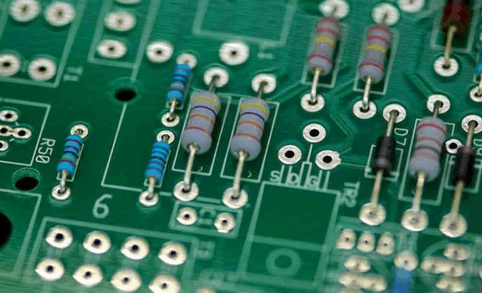
What is Circuit Board Stuffing?
Circuit board stuffing is a process of populating a printed circuit board (PCB) with electronic components. The process involves placing components onto the PCB in their respective positions and then soldering them onto the board. The components can be through-hole or surface mount, depending on the design of the PCB.
The process of circuit board stuffing can be done manually or by using automated machines. Manual stuffing is a time-consuming process that requires a skilled technician to ensure that the components are placed in the correct positions and soldered properly. Automated stuffing, on the other hand, is faster and more efficient, as it uses machines to place and solder the components.
Circuit board stuffing is a crucial step in the manufacturing of electronic devices. It is important to ensure that the components are placed and soldered correctly to ensure that the device functions properly. The process of circuit board stuffing can be complex, as it involves working with small components and intricate designs. However, with the right tools and techniques, it can be done efficiently and accurately.
The Circuit Board Stuffing Process
Component Preparation
Before beginning the circuit board stuffing process, it is important to prepare all the components that will be used. This includes identifying the correct components, checking their specifications, and verifying that they are in good working condition. It is also important to ensure that the components are properly labeled and sorted for easy identification during the stuffing process.
Board Preparation
Once the components are prepared, the circuit board must be prepared for stuffing. This involves cleaning the board to remove any dust or debris, and then applying a layer of flux to the board to help the solder adhere to the board. The board must also be checked for any defects or damage that could affect the stuffing process.
Component Placement
The next step in the circuit board stuffing process is to place the components onto the board in the correct positions. This can be done manually or with the use of automated placement machines. It is important to ensure that all components are placed in the correct orientation and at the correct distance from each other, as this will affect the performance of the circuit.
Soldering
The final step in the circuit board stuffing process is to solder the components onto the board. This involves heating the solder and applying it to the connection points between the components and the board. It is important to ensure that the solder is applied evenly and that all connections are properly made. After soldering, the board must be inspected to ensure that all connections are strong and secure.
Overall, the circuit board stuffing process is a critical step in the production of electronic devices. By following these steps and ensuring that all components are properly prepared, boards are properly cleaned and prepared, components are placed correctly, and soldering is done properly, the resulting circuit board will be of high quality and reliable performance.
Types of Circuit Board Stuffing
There are three main types of circuit board stuffing: Through-Hole, Surface Mount Technology (SMT), and Mixed Technology. Each type has its own advantages and disadvantages, and the choice of which to use will depend on the specific needs of the project.
Through-Hole Circuit Board Stuffing
Through-hole stuffing is the oldest and most traditional method of circuit board stuffing. It involves drilling holes in the board and inserting components through the holes, then soldering them in place on the opposite side of the board. Through-hole stuffing is best suited for larger components, such as connectors, switches, and electrolytic capacitors.
Advantages of through-hole stuffing include:
- Strong mechanical connections
- Easy to repair and modify
- Good for high-power applications
Disadvantages of through-hole stuffing include:
- Slower assembly time
- Limited to larger components
- Can be more expensive
Surface Mount Technology
Surface mount technology (SMT) is a newer method of circuit board stuffing that involves mounting components directly onto the surface of the board, rather than inserting them through holes. SMT components are much smaller than through-hole components, and are typically used for things like resistors, capacitors, and integrated circuits.
Advantages of SMT include:
- Smaller size, allowing for more compact designs
- Faster assembly time
- Lower cost
Disadvantages of SMT include:
- Weaker mechanical connections
- Harder to repair and modify
- Not suitable for high-power applications
Mixed Technology Circuit Board Stuffing
Mixed technology circuit board stuffing involves using both through-hole and SMT components on the same board. This allows designers to take advantage of the strengths of each type of stuffing. For example, through-hole stuffing can be used for high-power components, while SMT can be used for smaller, more compact components.
Advantages of mixed technology stuffing include:
- Flexibility to use the best stuffing method for each component
- Can reduce overall cost
- Can improve performance
Disadvantages of mixed technology stuffing include:
- More complex assembly process
- Requires more design planning
- Can be more difficult to troubleshoot
Overall, the choice of which type of circuit board stuffing to use will depend on the specific needs of the project. Designers should carefully consider the advantages and disadvantages of each method before making a decision.
Advantages of Circuit Board Stuffing
Increased Component Density
Circuit board stuffing enables the placement of more components on a board than traditional methods. This is because the process allows for components to be placed on both sides of the board, increasing the overall component density. By using smaller components and placing them closer together, the board can be made smaller and more efficient.
Improved Signal Integrity
Circuit board stuffing can improve signal integrity by reducing the length of signal traces. This is because components can be placed closer together, reducing the distance that signals have to travel. This can lead to a reduction in noise and interference, resulting in a more reliable and efficient circuit.
Reduced Size and Weight
Circuit board stuffing can reduce the size and weight of a circuit board. By placing components on both sides of the board, the overall size of the board can be reduced. This can be especially beneficial in applications where space is limited, such as in portable electronics.
Cost Savings
Circuit board stuffing can result in cost savings due to the reduced size and weight of the board. This can lead to lower material costs and reduced shipping costs. Additionally, the increased component density can reduce the number of boards required for a given application, further reducing costs.
In conclusion, circuit board stuffing offers several advantages over traditional methods, including increased component density, improved signal integrity, reduced size and weight, and cost savings.

Challenges and Considerations
Component Availability and Compatibility
One of the biggest challenges with circuit board stuffing is ensuring that all components are readily available and compatible with the board design. This can be a time-consuming process, as sourcing components from multiple vendors and verifying their compatibility can take a significant amount of effort.
To mitigate this challenge, it is important to work with trusted vendors who can provide reliable components in a timely manner. Additionally, it is important to carefully consider component compatibility during the design phase, to avoid any potential issues during the stuffing process.
Design for Manufacturability
Design for manufacturability (DFM) is an important consideration when it comes to circuit board stuffing. The design must be optimized for efficient and accurate assembly, while also ensuring that the final product meets the required specifications.
To achieve optimal DFM, it is important to work closely with the manufacturer throughout the design process. This can help identify any potential issues early on, allowing for adjustments to be made before the stuffing process begins.
Quality Control and Inspection
Quality control and inspection are critical components of any circuit board stuffing process. This ensures that the final product meets the required specifications and is free from defects.
To ensure effective quality control and inspection, it is important to establish clear guidelines and processes. This includes defining acceptable levels of defects, as well as establishing procedures for identifying and addressing any issues that arise during the stuffing process.
Overall, circuit board stuffing can be a complex process with a number of challenges and considerations to keep in mind. By carefully considering component availability and compatibility, design for manufacturability, and quality control and inspection, it is possible to achieve a successful outcome.
Comments are closed