A printed circuit board (PCB) is a crucial component in the electronics industry. It is responsible for connecting and controlling the various electronic components in a device. The development of PCBs has seen a significant advancement over the years, with the introduction of multi-layer PCBs being one of the most significant.
A 6-layer PCB prototype is a type of multi-layer PCB that has six layers of conductive material, separated by insulating layers. This type of PCB is commonly used in complex electronic devices that require a high level of connectivity and control. The additional layers allow for more circuitry to be added, making it more efficient and compact. The use of a 6-layer PCB prototype can also help to reduce the size of the device, making it more portable and convenient to use.
What is a 6 Layer PCB Prototype?
A 6 layer PCB prototype is a printed circuit board that consists of six layers of conductive material separated by insulating material. These layers are stacked on top of each other and connected through vias, which are small holes drilled through the layers.
The use of multiple layers allows for more complex circuit designs, as it provides additional space for routing traces and components. It also reduces the size of the board, making it more compact and easier to integrate into a product.
A 6 layer PCB prototype is commonly used in high-performance electronic devices, such as smartphones, computers, and medical equipment. It offers better signal integrity, reduced electromagnetic interference, and improved thermal management compared to a traditional 2 layer PCB.
Designing and manufacturing a 6 layer PCB prototype requires specialized knowledge and equipment. It involves creating a multilayer PCB stackup, selecting the appropriate materials, and ensuring that the layers are properly aligned and connected.
Overall, a 6 layer PCB prototype is a sophisticated and versatile solution for electronic circuitry that offers many benefits over traditional PCB designs.
Advantages of 6 Layer PCB Prototypes
Increased Design Flexibility
One of the major advantages of using a 6 layer PCB prototype is the increased design flexibility it provides. With more layers, designers have more options for routing and can create complex circuits without sacrificing space. This means that they can create smaller, more compact designs that are still highly functional.
Improved Signal Integrity
Another advantage of using a 6 layer PCB prototype is the improved signal integrity. With more layers, designers can separate power and ground planes, which reduces the noise and interference that can affect signal quality. This leads to better performance and reliability, which is especially important in high-speed applications.
Higher Component Density
Finally, a 6 layer PCB prototype allows for higher component density. With more layers, designers can place more components on the board without sacrificing performance or reliability. This is especially important in applications where space is at a premium, such as in portable devices or wearables.
In conclusion, a 6 layer PCB prototype offers increased design flexibility, improved signal integrity, and higher component density. This makes it an ideal choice for a wide range of applications, from consumer electronics to industrial automation.
Design Considerations for 6 Layer PCB Prototypes
Layer Stackup
The layer stackup for a 6 layer PCB prototype is a crucial design consideration. It is important to determine the number of signal layers, power planes, and ground planes needed for the design. A typical 6 layer PCB stackup includes two signal layers, two power planes, and two ground planes. The power and ground planes are placed adjacent to each other to minimize noise and provide a stable reference plane for signal layers.
Via Types and Placement
The via types and placement are also important considerations for a 6 layer PCB prototype. Blind vias and buried vias can be used to reduce the number of layers required for the design. It is important to ensure that the vias are placed in the correct location to minimize signal interference and maintain signal integrity.
Trace Width and Spacing
The trace width and spacing should be carefully considered to ensure that the design meets the required electrical specifications. The trace width should be wide enough to handle the required current without causing excessive resistance. The spacing between traces should be sufficient to prevent crosstalk and maintain signal integrity.
Copper Weight
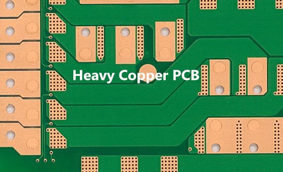
The copper weight is another important consideration for a 6 layer PCB prototype. The copper weight refers to the thickness of the copper on the PCB. A thicker copper weight can handle more current and provide better thermal management. However, a thicker copper weight can also increase the cost of the PCB.
In summary, designing a 6 layer PCB prototype requires careful consideration of layer stackup, via types and placement, trace width and spacing, and copper weight. By paying attention to these design considerations, you can ensure that your 6 layer PCB prototype meets the required electrical specifications and functions as intended.
Manufacturing Process for 6 Layer PCB Prototypes
Preparation of Copper Clad Boards
The first step in manufacturing a 6 layer PCB prototype is to prepare the copper clad boards. This involves cutting the boards to size and cleaning them to remove any dirt or impurities that could interfere with the bonding process.
Drilling and Plating of Through-Holes and Vias
Once the boards are prepared, the next step is to drill and plate through-holes and vias. This process involves drilling holes through the board and then plating them with a conductive material to create a connection between the layers.
Lamination and Bonding of Layers
After the through-holes and vias are plated, the layers are laminated and bonded together. This involves placing a layer of adhesive material between each layer and then applying heat and pressure to bond them together.
Etching and Plating of Inner Layers
Once the layers are bonded together, the next step is to etch and plate the inner layers. This involves removing unwanted copper from the surface of the board and then plating the remaining copper to create the circuit pattern.
Final Etching and Plating of Outer Layers
The final step in the manufacturing process is to etch and plate the outer layers. This involves removing the remaining unwanted copper from the surface of the board and then plating the remaining copper to create the final circuit pattern.
Overall, the manufacturing process for 6 layer PCB prototypes is a complex and precise process that requires careful attention to detail and a high level of expertise. By following these steps, manufacturers can create high-quality prototypes that meet the needs of their customers.
Testing and Quality Control for 6 Layer PCB Prototypes
To ensure the quality of 6 layer PCB prototypes, rigorous testing and quality control measures are necessary. The following sub-sections outline the various methods used to test and inspect 6 layer PCB prototypes.
Electrical Testing
Electrical testing is a crucial step in ensuring the functionality of a 6 layer PCB prototype. This testing involves checking for continuity, shorts, and open circuits. The following methods are used to perform electrical testing:
- Automated Optical Inspection (AOI)
- Flying Probe Testing
- In-Circuit Testing (ICT)

Visual Inspection
Visual inspection is an essential step in ensuring the quality of a 6 layer PCB prototype. This inspection involves checking for any defects that may have occurred during the manufacturing process. The following defects are checked during visual inspection:
- Soldering defects
- Component placement defects
- Copper trace defects
- Via hole defects
Dimensional Inspection
Dimensional inspection is necessary to ensure that the 6 layer PCB prototype meets the required specifications. This inspection involves checking the dimensions of the PCB, including the thickness, hole size, and copper thickness. The following methods are used to perform dimensional inspection:
- Digital calipers
- Micrometers
- Optical comparators
In conclusion, testing and quality control measures are essential to ensure the functionality and quality of 6 layer PCB prototypes. By performing electrical testing, visual inspection, and dimensional inspection, manufacturers can ensure that their 6 layer PCB prototypes meet the required specifications.
Comments are closed