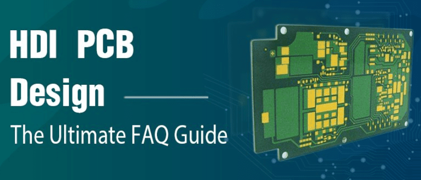
The PCB industry has undergone different changes in recent times, especially as they relate to the type of process technology used in making Printed Circuit Boards (PCBs). Today, the HDI technology is one of the sought-after and for good reasons.
Who would have imagined that a time would come when the entire electronics industry would follow the trends and make use of the relevant technologies? As MOKO Technology pointed out, the PCB market has undergone different changes, starting from the 1920s when the base for the modern circuit boards was laid.
It would soon be replaced by the “developing stages” between the early 1920s and the 1940s, when the printed circuit patterns were printed on a substrate of insulating, before the applications of the plaiting to make conductors for wiring.
Today, we have lots of process technologies for circuit board and the HDI process is one of the most popular.
What is the HDI PCB Manufacturing Process?
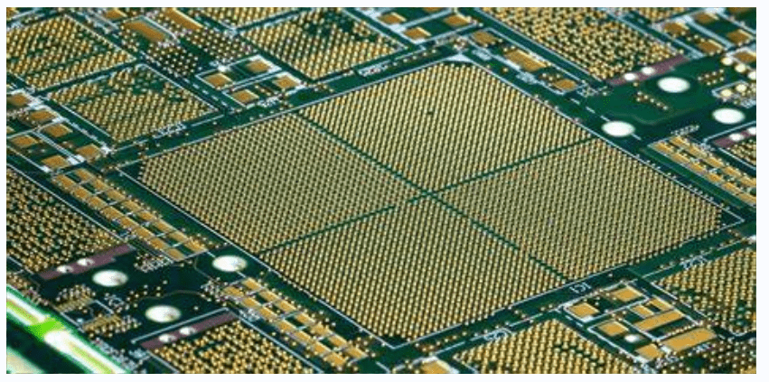
HDI stands for High Density Interconnect. It is so-called because of the composition of a higher wiring density per unit area. This higher wiring density per unit is one of the major advanced features that sets the HDI boards different from the traditional or standardized PCBs.
In this article, we discuss further about how the HDI PCB technology is a disruptor to the existing Printed Circuit Board (PCB) technology out there.
Correlating the HDI PCB Manufacturing Process to the Market Demand
It is expedient to mention that one of the major factors pushing the adoption of the High Density Interconnect (HDI) form of PCB design is the demands in the market.
There has been a steady shift in the electronics market, ranging from mobile devices to digital cameras. This shift centered on the need to make circuit boards smaller, while increasing the size of the components added therein.
Basically, the changes required the modification of the Printed Circuits Boards (PCBs) to weigh less and still have sufficient spaces to fit in the different electronic components. These changes also aimed at improving the electrical performance of the circuit boards.
It is against this backdrop that the HDI manufacturing process gained prominence, following the increased performance, including signal integrity, the increase in computational power and the packaging of multiple electronic circuitries in smaller packages.
You can think of the entire HDI technology as a means of maximizing the operations of your favorite electronics, without having to bother about complex wiring options and excessive weight.
Understanding the Higher Density Interconnector Terminologies
You need to understand that the HDI PCB design is subject to some processes and at the core of these processes are the distinct interconnect techniques that move the needle.
These are called the vias in pad and the micro vias. They are popular terms in the Printed Circuit Board (PCB) design process.
Here is a breakdown of how they function:
The Concept of “Vias”
Vias simply mean the interconnector or the medium through which the conductive pathways can be carved out on a PCB.
The process usually involves drilling holes into the Printed Circuit Board (PCB), which is why the Through Hole Technology (THT) became very popular. The drilled holes then provide a medium for the interconnections made for the different layers of a multilayer PCB.
Micro Vias
Out of the different types of vias used in circuit boards, the micro vias is mostly used with the HDI boards. It is a better competitor to the mechanical drilling or traditional drill bits used in conventional circuit boards.
Instead, the micro vias uses the laser drill format to pave the conductive pathways in the HDI board.
Despite the seemingly advantage over the mechanical drilling of traditional PCBs, laser drills can sometimes be problematic. The downside is that these vias are restricted to two layers only. Depending on how you go about it, the micro vias can either be staggered or used as a PCB stackup.
Blind Vias
This is another type of vias used in the PCB stackup. It works by creating a connection between the exterior or outer layers of a PCB, with the inner layers or interior layers. One benefit of this type of vias is that it terminates or stops at the inner layers, which makes it impossible for the end of the vias to be seen.
Buried Vias
The buried vias is an opposite of the blind vias in the sense that it doesn’t establish any connection with the external or outer layers. Instead, it only connects the internal layers and therefore, cannot be seen as they are “buried” inside the Printed Circuit Board (PCB).
Via In-Pad
In addition to having numerous properties, such as laser drilled vias, buried vias and blind vias, the HDI board also has many others stacked up. These include the use of the sequential lamination process and via in-pad.
The via in-pad is one of the consumer-driven processes for manufacturing circuit boards, in the sense that it allows for the integration of multiple technologies on fewer layers. The via in-pad process also supports the placement of the via directly within the pad that connects to the circuit component.
Below are some of the additional points you want to know about the via in-pad:
- More Components: multiple components can be integrated into the HDI PCB using the via in-pad because the pad supports that through the direct connection of the component lead to the internal layer of the circuit board.
- Improved Signal Integrity: the via in-pad process improves the signaling capability of the PCB by reducing the length of the signal path. This helps to remove the capacitive and the parasitic inductive defects. However, it is possible to remove or get rid of further signal reflections. Actualizing this would have to require the back drilling of the via in-pad, as a way of removing these signal reflections and in extension, improve the reliability of the signal coming from the HDI PCB.
Comparing the HDI Board Design to Traditional PCBs
There has been a debate on whether it is possible for the HDI boards to offer improved functionality than the traditional or the conventional circuit boards do. The answer is “yes.” It is possible for HDI PCBs to offer better features than the former PCBs.
Here are some of the ways that the HDI features prove to be more reliable than those of the traditional circuit boards:
1. The Density of the Component
Unlike the traditional PCBs that require lower component densities, the HDI PCB requires even more.
2. Device Optimizations
One of the core aspects of optimizing devices like mobile devices and laptop computers for circuit boards is the number of supported pins. Sometimes, the traditional PCBs might not be fully-compatible with both the high pin count devices, as well as the small pitch devices.
The reversal is the case with the HDI boards that are compatible with both the small pitch and the high pin count devices. With this level of device optimizations, you can be sure that more electronic devices can be optimized with the HDI printed circuit design process.
3. Vias Support
The types of vias used in a Printed Circuit Board (PCB) could impact the design outcome. Thus, the design rules have to be fully followed to get the best results.
Considering the changing trends in the Printed Circuit Board (PCB) technology, the trend is now giving way to inclusive vias process.
That is why the HDI board design towers above the traditional PCBs, in the sense that it supports the major vias types, such as the micro vias, the blind and buried vias.
By including the blind and buried vias, for instance, the HDI circuit board allows for flexible connections of the layers, in the sense that these layers can either be hidden or exposed. This is most especially for the outer layers of the board.
4. Circuit Board Sizing
The size of the circuit board depends largely on two factors – the board size and the weight. The components used therein also have a role to play.
Unlike the traditional PCBs that are bulkier, the HDI PCB’s board size is smaller and lighter because of the significant reductions in the sizes of the components.
5. Layering Procedures and Drilling Options
HDI PCBs use the laser drilling option, which helps improve the board’s heat resistance. In terms of the board layers, it typically supports fewer layers.
This is a sharp contrast to the multiple layers and the use of mechanical drilling options for the traditional circuit boards.
Benefits or Advantages of the High Density Interconnect (HDI) Manufacturing Process
One of the major reasons PCB hobbyists and consumers go for the High Density Interconnect (HDI) boards is because of what the name suggests – the densities are higher.
However, there are several other reasons why you should like this type of PCB. Below are some of the advantages:
Faster Circuit Production
Probably, one of the features you look for in a circuit board, aside from the number of densities, is the speed of production. Although the production timeframe might vary by the manufacturer, a bulk of the speedy design relies on the design rules of that PCB.
So, if you are working on a circuit board that is complex, you can expect to spend more time on it than on the one with less technicalities.
And that is one of the major advantages of the HDI PCBs. You don’t spend a lot of time figuring things because the stackup process is quite simplified. At the core is the ease of placing the components, which helps the manufacturer to speed up on other aspects such as testing the electrical performance and the high frequency transmission capability of the board.
HDI PCBs are Affordable
The affordability of circuit boards also plays an important role on the choose between one PCB and the other. In the case of the HDI PCBs, you can be sure to save a great deal of money, considering that the design process is straightforward.
Moreso, you don’t get to buy a lot of layers or invest in a lot of larger board sizes. Due to the reduced numbers of layers and the fact that multiple components can be integrated inside a smaller circuit board footprint; it makes it a lot easier for the HDI PCBs to be cheaper.
The HDI PCB Uses Smaller Aspect Ratios
The aspect ratio of the HDI PCBs give it a considerable edge over the traditional circuit boards. We must not fail to point out that a bulk of the reason for the lowered aspect ratio is because of the reduction in both the component pitch and size. That paves the way for more Input and Outputs (I/Os) in smaller geometries.
What’s more? The HDI PCB gains traction with its smaller aspect ratio because of the use of the micro vias, which has a better dependability or reliability than the traditional PCBs do. The outcome is that the micro vias significantly improved the plaiting of the vias, while allowing for an overall reliability in the transmission of signals.
That way, the HDI PCB wouldn’t be overly exposed to crossing delays and signal loss, which would have negatively impacted the high density interconnection.

Multiple Device Support
This is yet one other outstanding benefit of the HDI PCB design. It supports multiple devices, especially those small pitch devices, like the Ball Grid Array (BGA) components. These types of devices sometimes have 1 mm or less in pitch and they are not often supported in traditional PCBs.
HDI Boards have Compact Designs
It may have been expected that the support of higher densities could have required more board spaces for the HDI PCBs to function effectively.
That doesn’t appear to be the case because the HDI PCB works effectively, even with the smallest board size. This is possible because it conveniently reduces the numbers of layers and the sizes of the layers required to make a circuit board.
Shorter Signal Paths
Signals can be transmitted faster, only if there is a pathway that is not so restrictive. When you look at the signal paths of the traditional PCBs and that of the HDI PCBs, you can see the difference.
The HDI PCB has a defined signal path, which typically involves the use of the multiple via processes, most especially the micro vias and the via in-pad HDI manufacturing technology. The combination of these via processes helps the board to allow for more components to be placed in proximity to each other.
By design, the HDI components can be flexibly positioned, either by placing them on one side of the bare HDI PCB or by placing them on both sides of the PCB. That way, there would be adequate spacing and proximity that allows for the shortening of the signal paths. Thereby, the HDI PCB assures of an increase in the signal integrity, as well as the speedy transfer of these signals.
Heat Resistance is Top-Notch
The laser drilling method is commonly used in the HDI PCB, as a way of making (smaller) holes in the circuit board.
It is through these holes made with laser drilling that the HDI PCB can conveniently resist and dissipate heat faster.
Design Considerations for the High Density Interconnect (HDI) Board
There is no disputing the fact that the HDI PCB can improve signal reliability, save costs by way of reducing the layer count and design time. Yet, certain factors could possibly pose a challenge to the board design.
Here is a list of some of the design considerations and potential downsides you need to know before working with the HDI Printed Circuit Boards (PCBs):
Trace Capabilities
The trace capabilities of the HDI PCB can be limited. For example, the trace widths need extra attention for them to balance with the spacing limits on the board.
Second, there may be a need to use more trace routes. This is required to complete the board design. However, there is also the challenge that the longer the trace routes used in the HDI PCB, the longer it would take to transmit the signals.
Space Limitations
On the one hand, we have the spaces in the HDI PCB limited, so that the board can weigh less. On the other hand, PCB consumers tend to battle with the limitations created in the process, especially in terms of the limited workspace area on the board.
There is also the glaring limitation on the overt consideration for smaller components or more components that could fit into the tight or compacted spacing.
Applications of the HDI PCB
Where can one expect to use the HDI Printed Circuit Boards (PCBs)? Here is a list of some of the possible applications:
Aerospace Devices
HDI PCBs are used to manufacture the component parts, as well the electronic designs needed for the aerospace industry. Specifically, the electronic designs are targeted at the following:
- Defense applications
- Missile systems and;
- Aircraft applications
At the core of these applications is the fact that the HDI PCB helps to provide the reliable signal transmission, for which those applications need, especially in very extreme environmental conditions.
Automotive Market
The HDI Printed Circuit Boards (PCBs) are also used in the automotive industry, as a way of making the automotive electronics compact and lighter.
Consumer Electronics
Consumer devices, including laptop computers and smartphones have now been manufactured with HDI PCBs, because of the increased performance, lighter size and minimal space this type of PCBs does take.
The HDI Layout: How to Build a HDI PCB
Due to the streamlined pathway, the HDI PCB can be one of the simplest circuit boards to build. Yet, you must not ignore some of the important design iterations.
If you are to get the best results from your HDI PCB, you probably want to follow the following recommendations:
Layer Count Determination
One of the first things to do is to determine the layer count or the number of layers you need for the job. It must be noted that the layers are usually lower, but you want to be sure of the number for the design.
To calculate the layer count, you want to use either the interface plus direction from the largest Integrated Circuit (IC) on the board. You can also use the largest BGA components on the board.
Start Creating the HDI PCB Stackup
The next stage is to reach out to your PCB designer or manufacturer for both the dielectric data and the materials that would help you create the circuit board’s stackup.
Choose a Style for the Via
Depending on the type of via you choose, the number of layers on the board and the board’s thickness, you have to choose a style for positioning the via.
Note that the via style has to pave the way for an excellent routing density for the signals in the inner layers of the board.
Run some Tests
It is now time to be sure of how things would pan out. perform a reliability assessment test to be certain that the materials and the interconnects would function excellently. You also want to use the period to find out if the interconnects wouldn’t be damaged or subjected to fracture, especially during the assembling process.
Conform to Excellent HDI PCB Manufacturing Specifics
The design rules of the High Density Interconnect (HDI) made it possible for the board to accommodate multiple components, reduce the layer count and adapt to several applications.
Now, you don’t want to give it all up because of not paying attention to details. In addition to following the above design rules, you also need to conform to or follow the best practices for manufacturing the HDI PCBs.
Some of these best practices are clearances, the need for tear drops and trace widths.
Conclusion
Working with HDI Printed Circuit Boards (PCBs) exposes you to numerous opportunities that weren’t tenable in the traditional PCBs. These opportunities include but are not limited to the achievement of finer lines, reduction of the layers used in the board and excellent routing capabilities.
You also get to enjoy improved signal reliability, higher wiring density, and the use of multiple via processes to perfect component placements.
We have the knowledge and capability to take on your HDI PCB design project. Contact us today to get started.
Comments are closed