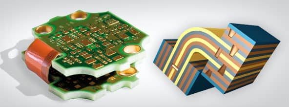
PCB boards are an essential component in modern electronic devices, and they play a crucial role in the functioning of these devices. PCB boards are made of a thin, flat material that is usually made of a combination of fiberglass and copper. These boards are designed to be rigid and durable, but they can also be bent to certain degrees without affecting their functionality.
Bending PCB boards has become a popular technique in recent years, particularly in the field of wearable technology. By bending PCB boards, manufacturers can create devices that are more flexible and comfortable to wear, without compromising on performance or durability. This technique has also been used in the development of foldable smartphones, which require flexible PCB boards to function properly. However, bending PCB boards requires careful planning and execution, as any mistakes can lead to damage or malfunction of the device.
What is a PCB Board?
A PCB (Printed Circuit Board) is a board made of non-conductive material that has conductive pathways etched onto its surface. These pathways are used to connect various electronic components together to form a functional circuit.
Components of a PCB Board
A PCB board is made up of several components, including:
- Substrate: A non-conductive material such as fiberglass or plastic that provides a base for the conductive pathways.
- Conductive pathways: These are thin traces of conductive material such as copper that run across the substrate and connect various components together.
- Components: These are electronic parts such as resistors, capacitors, and transistors that are connected to the conductive pathways to form a functional circuit.
- Solder mask: A layer of protective material that is applied to the surface of the board to prevent solder from flowing onto unwanted areas.
- Silkscreen: A layer of ink that is applied to the surface of the board to provide information such as component placement, part numbers, and other important details.
In conclusion, a PCB board is an essential component of electronic devices that allows for the creation of complex circuits in a compact and efficient manner. By understanding the components of a PCB board, you can gain a better understanding of how electronic devices work and how they are manufactured.
Bending PCB Boards
When it comes to printed circuit boards (PCBs), it’s not uncommon to need to bend them to fit into a specific enclosure or to conform to a specific shape. However, bending PCB boards can come with a few risks and considerations. In this section, we’ll explore the reasons for bending PCB boards and the associated risks.
Reasons for Bending PCB Boards
There are a few reasons why you might need to bend a PCB board:
- Enclosure requirements: If you’re designing a product that needs to fit into a specific enclosure, you might need to bend the PCB to fit the available space.
- Conformal coating: If you’re applying a conformal coating to your PCB, you might need to bend it to ensure that the coating covers all of the necessary components.
- Mechanical requirements: In some cases, a PCB might need to be bent to conform to a specific mechanical requirement, such as fitting around a curved surface.
Risks Associated with Bending PCB Boards
While bending PCB boards can be necessary, it’s important to consider the associated risks:
- Cracking or breaking: If a PCB is bent too far or too quickly, it can crack or break, rendering it unusable.
- Component damage: Bending a PCB can put stress on the components and potentially damage them.
- Solder joint failure: Bending a PCB can also put stress on the solder joints, which can lead to failure over time.
To minimize these risks, it’s important to follow best practices when bending PCB boards. This might include using a bending jig, gradually bending the board instead of trying to bend it all at once, and ensuring that the components and solder joints aren’t under too much stress.
Overall, while bending PCB boards can be necessary in some cases, it’s important to consider the associated risks and take steps to minimize them. By following best practices and taking a careful approach, you can ensure that your PCBs are bent safely and effectively.
Techniques for Bending PCB Boards
Manual Bending Techniques
Manual bending is the most common way to bend PCB boards. Manual bending is done by hand, using a bending tool or a plier. To bend a PCB board manually, follow these steps:
- Use a bending tool or plier to hold the board.
- Apply pressure to the board at the desired bend point.
- Slowly bend the board until it reaches the desired angle.
- Repeat the process for any additional bends.
Manual bending is a simple and cost-effective method for bending PCB boards. However, it requires a skilled operator to ensure that the board is not damaged during the bending process.
Automated Bending Techniques
Automated bending is a more advanced method of bending PCB boards. Automated bending is done using a machine that is programmed to bend the board at specific angles. To bend a PCB board using an automated machine, follow these steps:
- Load the board into the machine.
- Program the machine to bend the board at the desired angles.
- Activate the machine to begin the bending process.
- Remove the board from the machine once the bending process is complete.
Automated bending is a precise and efficient method of bending PCB boards. It is ideal for large-scale production and can significantly reduce production time and costs.
In conclusion, both manual and automated bending techniques have their advantages and disadvantages. The choice of which technique to use depends on the specific needs of the project and the available resources.
Factors to Consider
When bending PCB boards, there are several factors that need to be taken into consideration to avoid damaging the board or causing any defects. These factors include environmental, material, and design factors.
Environmental Factors
The environment in which the board is bent can have a significant impact on its overall quality. Temperature and humidity are two key factors that must be considered. High temperatures can cause the board to warp, while high humidity can cause the board to absorb moisture, leading to delamination or cracking. It is important to ensure that the bending process takes place in a controlled environment with stable temperature and humidity levels.
Material Factors
The material used to make the PCB board is also an important factor to consider when bending. The thickness and type of material used can affect the board’s flexibility and durability. Thinner boards are generally more flexible and easier to bend, while thicker boards may be more rigid and difficult to bend without causing damage. Additionally, the type of material used can affect the board’s ability to withstand bending without cracking or breaking.
Design Factors
The design of the PCB board also plays a role in its ability to be bent. The placement of components and the routing of traces can affect the board’s flexibility and strength. Components placed too close to the bend area can cause stress points, leading to cracking or breaking. Traces that are too close to the bend area can also cause stress points and weaken the board. It is important to design the board with the bending process in mind to ensure that it can be bent without causing any damage.

In conclusion, when bending PCB boards, it is important to consider environmental, material, and design factors to avoid damaging the board or causing any defects. By taking these factors into consideration, you can ensure that the bending process is successful and the board remains functional.
Conclusion
In conclusion, bending PCB boards can be a useful technique for certain applications, but it is important to approach it with caution and care. Here are some key takeaways to keep in mind:
- Bending PCB boards can be used to create custom shapes or fit into tight spaces, but it can also weaken the board and lead to failure if not done properly.
- It is important to follow best practices for bending, such as using a gradual curve and avoiding bending near components or traces.
- Consider the materials and thickness of the board when deciding whether or not to bend it.
- Always test the board thoroughly after bending to ensure it still functions properly.
- If you are unsure about whether or not to bend a PCB board, consult with a professional or do further research before proceeding.
Overall, bending PCB boards can be a useful technique in certain situations, but it should be approached with caution and care to avoid damaging the board or compromising its functionality. By following best practices and being mindful of potential risks, you can successfully bend PCB boards and achieve your desired results.
Comments are closed