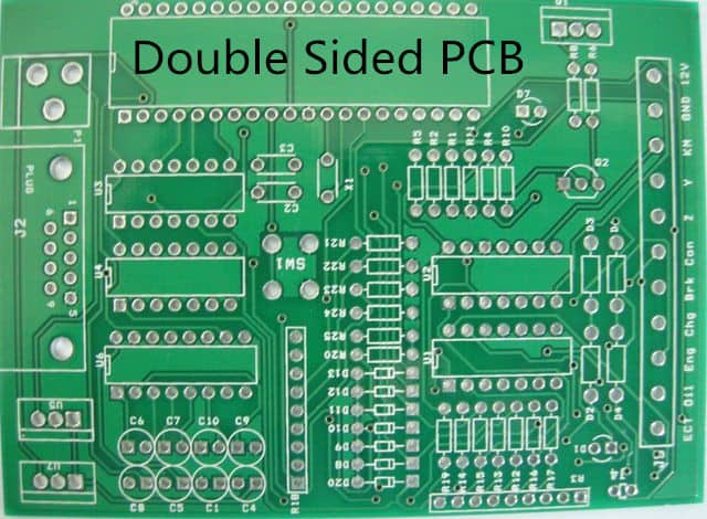
When it comes to the designing and the manufacturing of the Printed Circuit Boards (PCBs), the 2 Layer PCB is one of the options you can use.
The 2 Layer PCB is a type of Printed Circuit Boards (PCBs) that provides flexible accommodation of electrical components on the board. The 2 Layer PCB also helps to keep the board organized by striking the needed connection directly from the top layer to the bottom layer. It also provides enough space for the conductor patterns.
What Is the 2 Layer PCB?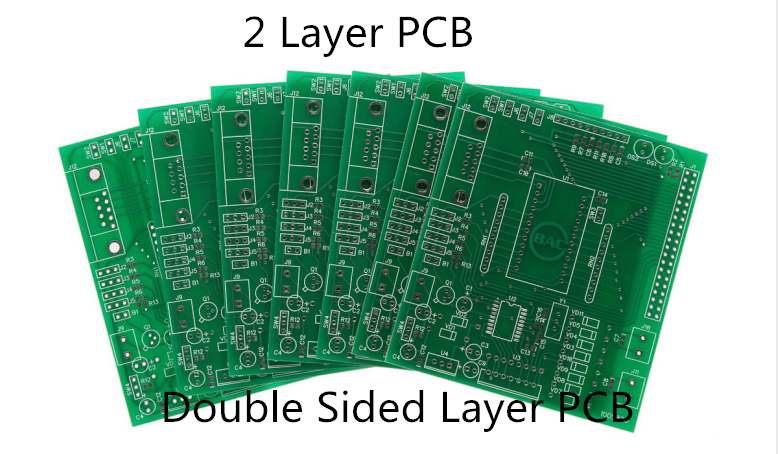
The 2 Layer PCB is a type of Printed Circuit Board (PCB) that has only two layers. We would also like to mention that although the 2 Layer PCB has more layers than the Single-Sided PCB (One Layer PCB), it doesn’t have more layers than the Multilayer PCB, which is where the 4 Layer PCB and the others fall into.
Second, the mass of the 2 Layer PCB makes it easier to have more layouts and surface for traces. Hence, the things that may not have been achieved in the Single-Sided PCB for want of space can be accomplished when using the 2 Layer PCB.
Third, the 2 Layer PCB provides more surface areas, which are ideal for housing the conductor pattern.
The fourth and most important point is that the 2 Layer PCB can be used in terms of mounting conductive copper and components on both sides of the PCB being worked on. The importance of this is that traces can cross over each other.
————————————————————-
Request 2 Layer PCB Manufacturing & Assembly Quote, Pls Send PCB File to Sales@raypcb.com Now
————————————————————-
Stack Up of the 2 Layer PCB
The 2 Layer PCB has a simplified stack up. This stack-up does not only make the task of layering it easier. It also helps to facilitate the completion of the design in good time.
So, what is the “special” stack up process that is being used on the 2 Layer PCB?
2 Layer PCB uses a Dual-Stack Up. This means that it only makes use of the primary components or layers, which are the Top Layer and the Bottom Layer.
Do I Need to Use a Ground Plane on Your 2 Layer PCB?
There are some consistent questions, which are being asked about the possibility of using Ground Planes on the 2 Layer PCB. Is it advised to use it?
We have looked at the potentiality of using the Ground Plane in your 2 Layer PCB, and came up with the submissions below:
- The Space Determines
Space or “real estate” you have available on your 2 Layer PCB should determine if you will integrate the Ground Plane.
Because there tends to be limited space on the 2 Layer PCB following the non-routing of signals through the internal signal layers, you may not have enough space left.
In this case, it is advised that you look for some space (if any) where the Ground Plane can be placed on the Printed Circuit Board (PCB).
Have in mind that if you are to mount or place the Ground Plane on your 2 Layer PCB, it has to be on one layer alone. So, you have to decide whether to place it on the Top Layer or the Bottom Layer.
Going by the name, it may ideal to place the Ground Plane on the Bottom Layer of your 2 Layer PCB.
- The Ground Plane Prevents Radiation
If you were successful at finding a space on the PCB for the Ground Plane, the next step is to start using it.
Ideally, one of the major advantages of having the Ground Plane on your 2 Layer PCB is that it helps to prevent radiation. It does this by providing some level of protection that tends to come from the EMI radiations.
- Placing the Ground Plane Close to Signal Traces
You can also take the placement of the Ground Plane to another level. This time, you are looking at placing it close to the signal traces.
If you do that, you can be sure that there will be limited EMI susceptibility and minimal inductances in the loop. This is bolstered by the fact that the return signals will have to closely follow the traces.
- Gridding
If you are not familiar with or you don’t want to use the placement of the Ground Plane to the Bottom Layer, you can use another option. This option is called “Gridding.”
It simply means that the Power and the Ground Traces can be routed in a way that they will not be interfering with each other’s operations.
Considering that this can give way to increase in noise, you have to do something about it. One of the things you can do here is to fill the empty spaces with Ground Pour.
————————————————————-
Request 2 Layer PCB Manufacturing & Assembly Quote, Pls Send PCB File to Sales@raypcb.com Now
————————————————————-
How Does the 2 Layer PCB Work?
There isn’t much to the 2 Layer PCB. It only needs to be placed in the right way to work accurately.
We must also mention that the 2 Layer PCB can function better if it is used alongside the microstrip traces and the ground planes.
If those are in place, the functionality of the 2 Layer PCB will be higher because there are little or no propagation delays to prevent it from working accurately.
The Design of the 2 Layer PCB
The 2 Layer PCB has a definite design. There are two angles to its design, and those have been discussed below.
- Vias’ Use
As you may have known, Printed Circuit Boards (PCBs) make use of vias for connectivity. This also becomes one of the strongest points of the 2 Layer PCB.
Here, the vias are primarily used to create the needed electrical connections. It is those connections that would, in turn, be used to route the traces until they get to the other side of the board.
- More Surface Area
The 2 Layer PCB is two times larger than the 2 Layer PCB. That means it has more spaces for additional components to be added.
To that end, the more surface area that is there provides just enough space for the inclusion of a conductor pattern.
2 Layer PCB vs. 4 Layer PCB
As earlier mentioned, the 2 Layer PCB is only one out of the many types of Printed Circuit Boards (PCBs). It comes after the Single-Sided PCBs, and after it, there is the Multilayer PCBs.
Most times, the 2 Layer PCB has been compared to the 4 Layer PCB, which happens to fall under the category of the Multilayer PCBs. The comparison is quite understandable considering that both types of PCBs (the 2 Layer PCB and the 4 Layer PCBs) have something in common.
From the use of the top and the bottom layers to the medium of connections, the 2 Layer PCB and the 4 Layer PCB are often compared.
Despite the comparison, some factors still come into play to distinguish the 2 Layer PCB from the 4 Layer PCB.
————————————————————-
Request 2 Layer PCB Manufacturing & Assembly Quote, Pls Send PCB File to Sales@raypcb.com Now
————————————————————-
How to Choose Your 2 Layer PCB
So, you are intent on designing your first 2 Layer PCB. That is a commendable move.
However, we want you to know some things before you proceed. These factors will help you in making a decision on how to select or choose your next 2 Layer PCB.
Here are the things you need to put into consideration:
- Lead Time
The Lead Time is similar to “how fast” the 2 Layer PCB can be designed. It might interest you to know that 2 Layer PCBs have one of the fastest Lead Times. Ideally, the board can be shipped within 24 hours (1 day) from the time of receipt.
- Level of Functionality
The 2 Layer PCB is between simplicity and complexity. If you can perfectly design One Layer (Single-Sided PCB), you may not have some trouble with the 2 Layer PCB.
Nonetheless, you may enlist the services of a PCB manufacturer to help you with the project.
Aside from that, you have to consider the functionality of the 2 Layer PCB. If it is more complex, you may have to start considering using the 4 Layer PCB.
- Budget/Cost
The cost has always been an influential factor in the selection of 2 Layer PCB. For good reasons, you can leverage this.
This is because the 2 Layer PCB doesn’t dip many holes in your pocket the way the 4 Layer PCB does.
Therefore, if you are looking at getting your Printed Circuit Board (PCB) done without breaking the bank, the 2 Layer PCB is your sure bet.
- Dimension/Size
What is the size or the maximum dimension you expect of your Printed Circuit Board (PCB)?
Ideally, the 2 Layer PCB has a maximum board size/dimension of 650x520mm. So, if your expectation is above that, you want to consider the 4 Layer PCB with a maximum dimension of 650x500mm.
Wrapping Up
The 2 Layer PCB proves to be one of the cost-effective, flexible, spacious (than the Single-Sided PCB), and a PCB with one of the fastest lead time.
You want to make use of a PCB manufacturer that has many years of experience working at the 2 Layer PCB because that is a guarantee that your project is in safe hands.
Comments are closed