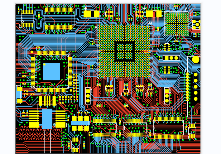
The use of software for PCB design has become an increasing practice in recent times. Cadence PCB is one such software you don’t want to miss using. It helps you structure the circuit board designs, while balancing the performance of the design iterations with collaborative support.
If you have always wanted to know if choosing Cadence PCB is a good choice or not, this article should help you gain clarity.
What is Cadence PCB?
It is a Printed Circuit Board (PCB) design tool or software. It has one goal – to make the designs of circuit boards simpler.
It is to be mentioned that the Cadence PCB solutions are geared towards the removal of bottlenecks in the automated PCB design process, whereby the designers end up using the wrong commands or making mistakes that eventually lead to several revisions. Such instances defeat the purpose of software usage, which is to simplify the design iterations and make the output unique.
Simulation-Driven Solutions and Other Cadence PCB Benefits
One of the major benefits of using the Cadence PCB software is the usage of simulation-driven solutions, which go a long way to bolster the integration of complete and integrated solutions for the entire electronic product design process.
The following are some of the additional reasons or benefits of using the Cadence PCB software:
1. Extensive Product Library
The Cadence PCB software covers a broad range of product categories, ranging from the front-end schematic capture to the combination of the analog and mixed signal simulations.
The product categories also cover the following:
- SI/PI Analysis Point Tools
- Back-end Board Layout and Routing
- Library and Design Data Process Management
2. Collaborative PCB Designs
How would you like partnering or collaborating with your team to get the job done? That is one of the huge benefits of working with the Cadence PCB software – collaborative designs.
This feature allows the circuit board designers to share ideas in real-time, while maximizing the functions of the software to complete the PCB project.
Below are some of the additional benefits of the Collaborative PCB design concept:
- Design Rule Implementation: both the design rules and design goals are noted and implemented throughout the process. That way, the designers don’t get a chance to deviate from the original process or make mistakes.
- Extensive Collaborations: the collaborative tendencies of the Cadence PCB software are not limited to in-person or one-on-one partnership. Instead, the designers get to leverage the extensive collaboration options, ranging from “across the wall” and design domains.
- Complex Board Designs: the real-time collaborative design also allows the users to work on both the single circuit boards and the complex, multi-board Printed Circuit Board (PCB) systems.
Cadence PCB & Analysis Technology
Cadence PCB uses an extensive portfolio of process technologies to deliver on the promise of simplifying the circuit board design process.
At the core of the process technologies is the Allegro Right First-Time Design, which allows for the avoidance of late-stage design changes, as well as the reworks for mistakes. The design process also allows for the introduction of real-time design rule verification, which helps the designers to keep an eye on the process as they design the circuit boards.
The following are some of the additional industry-leading technologies Cadence PCB uses to solve many PCB design challenges:
Augmented Reality Lab Tools
These are dedicated tools designed to help you facilitate, debug, rework and assemble the Printed Circuit Boards (PCBs) in the shortest time possible. It is to be also mentioned that these tools are optimized for the highest performance levels, especially as they help reduce the chances of making mistakes.

Sigrity Serial Link Analysis
Some PCBs, after design, begin to perform contrary to expectations. It is for this reason that Cadence PCB uses a process technology called Sigrity Serial Link Analysis. The objective is to help the designers check the compliance of all the sections of the multi-gigabit serial links.
With that in place, the chances of having underperforming PCBs will be greatly reduced.
Allegro TimingVision Environment
It is also possible that the PCB will “escape” some checks and on release, will underperform. It is for this reason that Cadence PCB introduced a technology called the Allegro TimingVision Environment.
The function is to detect timing issues, as well as make real-time visual feedback that would help in addressing these issues on time.
Constraint-Driven PCB Layout
This is a dedicated process to the layout process of Printed Circuit Boards (PCBs). One of the major reasons why this is important is that it helps to reduce the hassles that come with making changes to already-finished circuit boards.
At the core of the functionality is the use of a constraint-driven architecture that provides the common, yet consistent system upon which the circuit boards can be designed with ease. Some of the attributes include the creation, management and the validation of the constraints, both from the front and back.
The major benefit to this process is that it helps eliminate the additional time to be spent in correcting the mistakes. In extension, this also translates the shorter lead times.
Cadence PCB Solutions
Below is a breakdown of the different solutions offered by Cadence PCB:
3D System Design Solutions
The introduction of the 3D System Design Solutions is designed to bolster the visualization of the complex high-speed systems and the simulation of the signal integrity for the signal and return the paths to packages and dies.
Multi-Board Design
The Cadence PCB solutions also cover the design of complex and multi-board circuits. This is in place to ensure the removal of the irrelevant system re-spins, as well as to bolster the connectivity options for the PCBs
IC/Package/PCB Co-Design
Just like the collaborative design process, the IC/Package/PCB Co-Design is designed to be a medium through which circuits can be scaled in good time.
It supports cross-domain planning in a single design tool. This then enables the use of shorter cycle times when working on the high-performance interfaces.
Wrapping Up
While the Cadence PCB software proves to be one of the best in terms of collaborative working and seamless integrations, it is also compared to other tools.
One of the major comparisons is that of Cadence PCB to the OrCAD. It is to be noted that the two belong to the broader Cadence PCB suite, whereby the Allegro is used for PCB layout purposes, while the OrCAD is used as a schematic capture tool for circuit boards.
Comments are closed