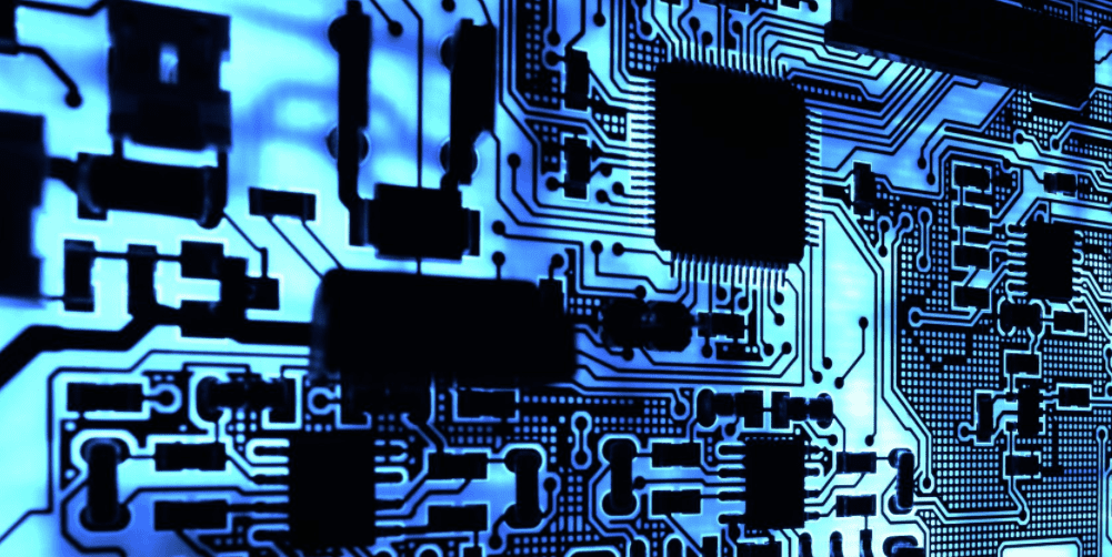
Simple circuit PCB design is a crucial aspect of electronic engineering. PCB design is the process of creating a printed circuit board that connects electronic components using conductive tracks, pads, and other features. Simple circuit PCB design is particularly important for beginners who are learning the basics of electronic engineering.
A simple circuit board design typically involves designing a circuit that is easy to understand and build. This usually involves using a small number of components, such as resistors, capacitors, and transistors. The circuit should also be easy to manufacture, which means that the design should be optimized for efficient use of space and minimal use of materials. In addition, the design should be tested thoroughly to ensure that it works as intended.
Basics of Simple Circuit PCB Design
Understanding PCB Design
PCB stands for Printed Circuit Board. PCB design is the process of designing and laying out the physical circuit board that connects electronic components. A PCB is a board made of insulating material such as fiberglass or plastic, with conductive pathways etched onto its surface. These pathways are used to connect components such as resistors, capacitors, and transistors.
The design of a PCB involves several steps, including schematic capture, layout design, and fabrication. Schematic capture is the process of creating a diagram that shows how the components are connected. Layout design involves placing the components on the board and routing the connections between them. Fabrication involves creating the physical board from the design files.
Components of a Simple Circuit PCB Design
A simple circuit PCB design typically consists of a few basic components, including resistors, capacitors, transistors, and power sources. Resistors are used to limit the flow of current in a circuit. Capacitors store electrical charge and can be used to filter out unwanted noise. Transistors are used to amplify or switch electrical signals.
Power sources can come in many forms, including batteries, wall outlets, and solar panels. When designing a simple circuit PCB, it is important to choose the appropriate power source for the application.
In addition to these basic components, there are many other components that can be used in a simple circuit PCB design, including diodes, inductors, and sensors. The choice of components will depend on the specific application and the desired functionality of the circuit.
Overall, understanding the basics of simple circuit PCB design is essential for anyone interested in electronics or engineering. By following the proper design process and selecting the appropriate components, it is possible to create functional and reliable circuits for a wide range of applications.
Designing a Simple Circuit PCB
Schematic Capture
The first step in designing a simple circuit PCB is to create a schematic capture. A schematic is a visual representation of the circuit, showing how the components are connected to each other. There are many software tools available to create schematics, such as Eagle, KiCad, and Altium Designer.
When creating a schematic, it is important to ensure that the components are correctly connected and that all necessary components are included. It is also a good practice to label all components and connections for clarity.
PCB Layout Design
Once the schematic is complete, the next step is to design the PCB layout. The layout is the physical representation of the circuit board, showing the placement of components and their connections. The layout should be designed with consideration for the size and shape of the board, as well as any constraints on the design, such as the need to fit into a particular enclosure.
When designing the layout, it is important to consider factors such as signal integrity, power distribution, and thermal management. The layout should be optimized to minimize noise and interference, and to ensure that power is distributed evenly across the board.
Routing the PCB
The final step in designing a simple circuit PCB is to route the board. Routing involves creating the physical connections between components on the board. This is typically done using automated routing software, which can optimize the routing for factors such as signal integrity and thermal management.
When routing the board, it is important to consider factors such as the length of the traces, the number of vias required, and the placement of components. The routing should be optimized to minimize noise and interference, and to ensure that the board is reliable and easy to manufacture.
In conclusion, designing a simple circuit PCB requires careful planning and attention to detail. By following the steps outlined above, it is possible to create a reliable and effective PCB for a wide range of applications.
PCB Manufacturing
Printing the PCB Design
The first step in PCB manufacturing is to print the PCB design onto a copper-clad board. This can be done using a laser printer and special transfer paper, or by using a photoresist process. The transfer paper or photoresist is then placed onto the copper-clad board and exposed to UV light. This causes the design to be transferred onto the board.
Etching the PCB
Once the design is printed onto the copper-clad board, the next step is to etch away the unwanted copper. This is typically done using a chemical etchant, such as ferric chloride. The board is dipped into the etchant, which dissolves the copper that is not protected by the transferred design. After the etching is complete, the board is rinsed and dried.
Drilling and Plating
After the PCB has been etched, it is time to drill the holes for the components. This is typically done using a CNC machine. Once the holes are drilled, the board is plated with a thin layer of metal, such as copper or gold, to protect the traces and pads from oxidation. This plating process is typically done using an electroplating process.
Overall, PCB manufacturing is a complex process that requires precision and attention to detail. By following the proper steps and using high-quality materials, it is possible to create PCBs that are reliable and durable.
Testing and Troubleshooting

Testing the PCB
After designing a simple circuit PCB, it is essential to test it before using it in a project. Testing the PCB helps to ensure that it is functional and meets the intended specifications. The following steps can be followed to test a PCB:
-
Visual Inspection: Inspect the PCB for any visible defects or errors, such as incorrect component placement or soldering issues.
-
Continuity Testing: Use a multimeter to check for continuity between the power and ground pins and other critical points on the PCB.
-
Functional Testing: Connect the PCB to a power source and test its functionality using an oscilloscope or logic analyzer.
Troubleshooting Common Issues
Even after thorough testing, PCBs can still encounter issues. Here are some common issues and their potential solutions:
-
Short Circuits: If a short circuit is detected, check for any loose or misplaced components, and fix any soldering issues.
-
Open Circuits: If an open circuit is detected, check for any broken or disconnected traces or components, and repair them.
-
Component Failure: If a component fails, replace it with a new one.
-
Noise and Interference: If noise or interference is detected, check for any grounding issues or signal integrity problems.
In conclusion, testing and troubleshooting are critical steps in the PCB design process. By following these steps and addressing any issues that arise, the PCB can be made functional and reliable.
Comments are closed