Printed circuit board designers are the unsung heroes behind the electronic devices we use every day. They are responsible for designing the intricate circuitry that allows our smartphones, laptops, and other gadgets to function. Without their expertise, these devices would not be able to perform the complex tasks we rely on them for.
Printed circuit board designers use specialized software to create the layout of the circuitry, determine the placement and routing of components, and ensure that the design meets the required specifications. They work closely with engineers and other professionals to ensure that the design is optimized for performance, reliability, and cost-effectiveness. In addition, they must stay up-to-date with the latest technologies and industry standards to ensure that their designs are cutting-edge and meet the needs of their clients.
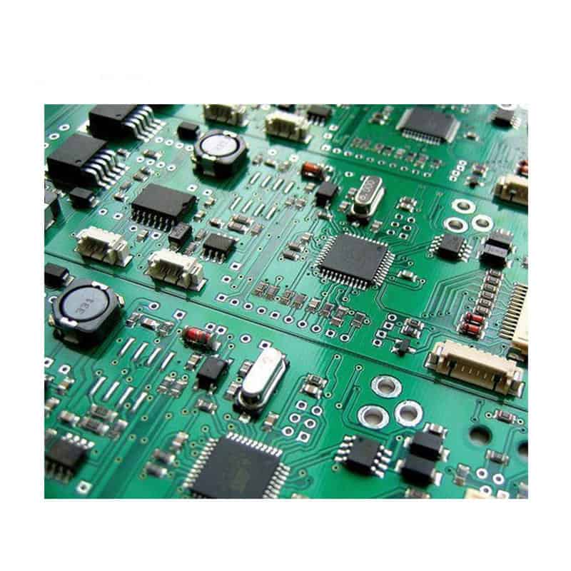
The Role of Printed Circuit Board Designers
Responsibilities
Printed Circuit Board (PCB) designers are responsible for designing and testing electronic components that are used in a wide range of products, from computers and smartphones to medical devices and aerospace equipment. They work closely with engineers and technicians to develop the layout and design of the circuit boards, ensuring that they meet the required specifications and standards.
Some of the key responsibilities of PCB designers include:
- Collaborating with engineers and technicians to understand the requirements and specifications of the project.
- Designing and testing the layout of the circuit board using specialized software.
- Ensuring that the circuit board meets the required standards and regulations.
- Troubleshooting and resolving any issues that arise during the design and testing process.
- Providing technical support to other members of the team.
Skills
To be an effective PCB designer, you need to have a range of technical and interpersonal skills. Some of the key skills required for this role include:
- Proficiency in specialized software such as Altium Designer or Cadence Allegro.
- Strong knowledge of electronics and circuit board design principles.
- Attention to detail and the ability to work accurately and efficiently.
- Excellent problem-solving skills and the ability to troubleshoot issues.
- Strong communication and interpersonal skills to work effectively with other members of the team.
Qualifications
Most PCB designers have a degree in electrical engineering or a related field. However, some employers may also consider candidates with a diploma or certificate in electronics or a related field, provided they have relevant experience and skills.
In addition to formal qualifications, PCB designers also need to keep up to date with the latest industry trends and developments. This may involve attending training courses, conferences, and seminars, as well as participating in online forums and communities.
Overall, PCB designers play a critical role in the development of electronic components and products. Their expertise and skills are essential to ensuring that these products are safe, reliable, and meet the required standards and regulations.
The Design Process
Designing a printed circuit board (PCB) is a complex process that requires a thorough understanding of the design requirements, electronic components, and manufacturing processes. The design process can be divided into three main stages: schematic design, layout design, and design verification.
Schematic Design
In the schematic design stage, the designer creates a graphical representation of the circuit using a schematic capture tool. The schematic shows the interconnection of the components and their functions. The designer must ensure that the circuit meets the design requirements and that all components are compatible with each other.
Layout Design
In the layout design stage, the designer creates a physical representation of the circuit board. The designer must place the components on the board and route the traces to connect them. The designer must also consider the physical constraints of the board, such as size, shape, and mounting holes. The layout design must ensure that the circuit meets the design requirements and that it can be manufactured with high yield.

Design Verification
In the design verification stage, the designer checks the design for errors and verifies that it meets the design requirements. The designer must perform electrical and physical checks to ensure that the circuit works as intended and that it can be manufactured with high yield. The designer must also consider the environmental and safety requirements of the circuit.
In conclusion, the design process is a critical part of PCB design. The designer must have a thorough understanding of the design requirements, electronic components, and manufacturing processes. The designer must also ensure that the circuit meets the design requirements and can be manufactured with high yield.
Tools and Software
Printed circuit board designers rely heavily on a variety of software tools to create and test their designs. The two main categories of software used in PCB design are CAD software and simulation software.
CAD Software
CAD software is used to create the layout and design of a printed circuit board. Some of the most popular CAD software tools used by PCB designers include:
- Altium Designer
- Eagle PCB Design
- KiCad
- OrCAD PCB Designer
- PADS PCB Design
Each of these tools has its own unique features and capabilities, so designers often choose the one that best suits their needs and preferences.
Simulation Software
Simulation software is used to test and verify the functionality of a PCB design before it is manufactured. This software allows designers to simulate various scenarios and identify potential issues before they occur. Some of the most commonly used simulation software tools for PCB design include:
- LTspice
- Proteus
- Simulink
- SPICE
Simulation software is an essential tool for ensuring that a PCB design will work as intended and meet the necessary requirements.
In addition to CAD and simulation software, PCB designers also use a variety of other tools and resources, such as:
- Schematic capture tools
- PCB layout tools
- Design rule checkers
- Signal integrity analysis tools
- 3D modeling software
By using these tools and resources, PCB designers are able to create high-quality, functional designs that meet the needs of their clients and end-users.
Design Considerations
When designing a printed circuit board (PCB), there are several important considerations that must be taken into account. Here are some of the key design considerations that PCB designers should keep in mind:
Signal Integrity
Signal integrity is crucial in ensuring that the signals being transmitted through the PCB are clean and free from interference. To achieve good signal integrity, designers must consider factors such as trace length, impedance matching, and noise reduction techniques.
Designers can use simulation tools to analyze and optimize the signal integrity of their PCB designs. It is important to note that signal integrity is not just a concern for high-speed digital circuits, but also for analog circuits.
Power Integrity
Power integrity is essential in ensuring that the power supply to the PCB is stable and free from noise. Designers must consider factors such as power plane design, decoupling capacitor placement, and power distribution network (PDN) analysis.
Designers can use simulation tools to analyze and optimize the power integrity of their PCB designs. It is important to note that power integrity is not just a concern for high-power circuits, but also for low-power circuits.
Thermal Management
Thermal management is critical in ensuring that the components on the PCB do not overheat and fail. Designers must consider factors such as component placement, heat sink design, and thermal vias.
Designers can use simulation tools to analyze and optimize the thermal management of their PCB designs. It is important to note that thermal management is not just a concern for high-power circuits, but also for low-power circuits.
In conclusion, signal integrity, power integrity, and thermal management are all important considerations that PCB designers must keep in mind when designing their PCBs. By carefully considering these factors, designers can ensure that their PCBs are reliable and perform as intended.
Manufacturing and Assembly
When it comes to manufacturing and assembly of printed circuit boards (PCBs), there are two important considerations: Design for Manufacturability (DFM) and Design for Assembly (DFA).
Design for Manufacturability
DFM is the process of designing a PCB to be easily and efficiently manufactured. This involves taking into account the capabilities and limitations of the manufacturing equipment and processes, as well as the materials used. By designing for manufacturability, PCB designers can reduce the cost and time required for production, while also improving the overall quality and reliability of the PCB.
Some key considerations for DFM include:
- Component placement: Placing components in a way that allows for efficient assembly and reduces the risk of errors or defects.
- Trace and space: Ensuring that the spacing between traces and components is appropriate for the manufacturing process and materials used.
- Layer stackup: Choosing an appropriate layer stackup that balances cost, performance, and manufacturability.
- Panelization: Arranging PCBs on a panel to maximize the use of manufacturing equipment and reduce waste.
Design for Assembly
DFA is the process of designing a PCB to be easily and efficiently assembled. This involves taking into account the capabilities and limitations of the assembly equipment and processes, as well as the skills and experience of the assembly technicians. By designing for assembly, PCB designers can reduce the risk of errors or defects during assembly, while also improving the overall quality and reliability of the PCB.
Some key considerations for DFA include:
- Component selection: Choosing components that are easy to handle and assemble, and that are compatible with the assembly process and materials used.
- Soldering: Ensuring that the soldering process is appropriate for the components and materials used, and that the solder joints are strong and reliable.
- Testing: Designing the PCB in a way that allows for easy and effective testing of the finished product, to ensure that it meets the required specifications.
In summary, designing for manufacturability and assembly is essential for creating high-quality and cost-effective PCBs. By taking into account the capabilities and limitations of the manufacturing and assembly processes, PCB designers can improve the efficiency, reliability, and overall performance of their designs.
Testing and Troubleshooting
Functional Testing
Once the Printed Circuit Board (PCB) has been assembled, it is essential to test its functionality. Functional testing involves verifying that the PCB performs as expected and meets the design requirements.
One way to perform functional testing is to use a test fixture or bed-of-nails tester. The test fixture is designed to hold the PCB in place and provide access to all the test points. The bed-of-nails tester has a series of pins that make contact with the test points on the PCB. The tester then applies power and signals to the PCB and verifies that the output is correct.

Debugging
If the functional test fails, the next step is to debug the PCB. Debugging involves identifying the root cause of the problem and fixing it.
One way to debug the PCB is to use an oscilloscope or logic analyzer. These tools allow the designer to monitor the signals on the PCB and identify any anomalies. Once the problem has been identified, the designer can then make the necessary changes to fix it.
Repair
If the PCB has a defect, it may need to be repaired. Repair involves fixing the defect without damaging the rest of the PCB.
One way to repair a PCB is to use a soldering iron and solder wick. The solder wick is used to remove the excess solder from the PCB, and the soldering iron is used to add new solder to the PCB. This process requires a steady hand and good soldering skills.
In summary, testing and troubleshooting are critical steps in the PCB design process. Functional testing ensures that the PCB meets the design requirements, while debugging and repair are necessary to fix any issues that arise.
Comments are closed