Computer printed circuit boards, or PCBs, are a vital component of modern electronic devices. They are used to connect and control the flow of electricity between various electronic components, such as microprocessors, memory chips, and sensors. PCBs are essential for the proper functioning of devices ranging from smartphones and laptops to cars and airplanes.
PCBs are typically made of a thin layer of copper foil, which is etched with a pattern of circuitry to create the desired electrical connections. The copper layer is then laminated onto a non-conductive substrate, such as fiberglass or plastic, to create a rigid board. PCBs can be single-sided, with circuitry on only one side of the board, or double-sided, with circuitry on both sides. More complex devices may require multi-layer PCBs, which contain multiple layers of circuitry separated by insulating layers.
What is a Computer Printed Circuit Board?
A computer printed circuit board (PCB) is a thin board made of insulating material that houses electronic components and provides electrical connections between them. It is an essential component of modern electronic devices, including computers, smartphones, and other electronic gadgets.
Functionality of a Computer Printed Circuit Board
The primary function of a PCB is to provide a platform for electronic components to be mounted and connected. The board is designed with a series of conductive pathways, known as traces, which connect the components and allow electricity to flow between them. These traces are made from copper or other conductive materials and are etched onto the surface of the board.
PCBs are typically made using a process known as surface-mount technology (SMT), which involves placing components directly onto the surface of the board. This method allows for smaller and more compact designs, making it ideal for use in portable electronic devices.
In addition to providing a platform for electronic components, PCBs also offer several other benefits. They help to reduce the size and weight of electronic devices, improve their reliability, and reduce the risk of electrical interference.
Overall, the computer printed circuit board is a critical component in modern electronic devices, providing a platform for electronic components to be mounted and connected while also offering several other benefits.
Types of Printed Circuit Boards
There are three main types of printed circuit boards (PCBs): single-sided, double-sided, and multi-layer. Each type has its own advantages and disadvantages, and the choice of PCB type depends on the specific application and requirements.
Single-Sided PCBs
Single-sided PCBs are the simplest type of PCB. They have only one layer of conductive material, usually copper, on one side of the board. The other side of the board is usually coated with a non-conductive material, such as epoxy or fiberglass.
Single-sided PCBs are the most cost-effective type of PCB, and they are commonly used in simple electronic devices, such as calculators and remote controls. However, they have limited functionality and are not suitable for complex circuits.
Double-Sided PCBs
Double-sided PCBs have two layers of conductive material, one on each side of the board. The layers are connected by vias, which are small holes drilled through the board and filled with conductive material.
Double-sided PCBs are more versatile than single-sided PCBs and can be used in a wider range of applications. They are commonly used in consumer electronics, such as smartphones and laptops.
Multi-Layer PCBs
Multi-layer PCBs have three or more layers of conductive material, separated by layers of insulating material. The layers are connected by vias, which allow the circuits to pass through the different layers.
Multi-layer PCBs are the most complex type of PCB, and they are used in high-performance electronic devices, such as servers and medical equipment. They offer better signal integrity, reduced electromagnetic interference, and higher density of components.
In conclusion, the choice of PCB type depends on the specific application and requirements. Single-sided PCBs are the most cost-effective but have limited functionality, while double-sided PCBs are more versatile and commonly used in consumer electronics. Multi-layer PCBs are the most complex and used in high-performance electronic devices.
Designing a Printed Circuit Board
Schematic Design
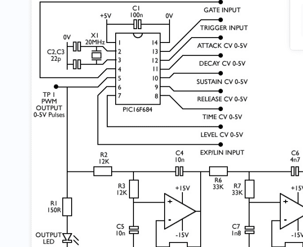
The first step in designing a printed circuit board (PCB) is to create a schematic diagram. This is a graphical representation of the circuit that shows how the components are connected. There are many software tools available for creating schematics, such as Eagle, KiCAD, and Altium Designer.
When creating a schematic, it is important to follow some best practices, such as using consistent symbols and labels, keeping the design simple, and minimizing the use of vias and crossovers. It is also important to ensure that the schematic is complete and accurate, as any errors or omissions can cause problems in the final PCB.
Layout Design
Once the schematic is complete, the next step is to create the PCB layout. This involves placing the components on the board and routing the traces that connect them. There are many factors to consider when designing the layout, such as the size and shape of the board, the placement of components, and the routing of traces.
To ensure a successful layout, it is important to follow some best practices, such as keeping the traces as short and direct as possible, avoiding right angles and acute angles, and minimizing the use of vias. It is also important to consider the manufacturing process, as some designs may be more difficult or expensive to manufacture than others.
Manufacturing Process
Once the layout is complete, the final step is to manufacture the PCB. This involves several steps, such as printing the layout onto a copper-clad board, etching away the unwanted copper, drilling holes for the components, and applying a solder mask and silkscreen.
There are many factors to consider when manufacturing a PCB, such as the choice of materials, the thickness of the board, and the quality of the solder mask and silkscreen. It is also important to follow some best practices, such as ensuring that the board is properly cleaned and inspected before and after assembly, and using a suitable soldering technique for the components.
Overall, designing a printed circuit board requires careful planning and attention to detail. By following some best practices and considering the manufacturing process, it is possible to create a high-quality and reliable PCB that meets the needs of the application.
Advantages of Printed Circuit Boards
Cost-effective
Printed Circuit Boards (PCBs) are cost-effective compared to traditional wiring methods. PCBs are designed to minimize the use of wires and components, reducing the overall cost of production. PCBs are also easier to assemble, reducing labor costs. With the advancement of technology, PCBs can now be produced in large quantities at a lower cost, making them an ideal choice for mass production.
Compact Size
PCBs are designed to be compact and take up less space than traditional wiring methods. This is because PCBs are made up of layers of conductive materials that are printed onto a board. The layers are then laminated together to form a single board. This allows for more components to be placed onto a single board, reducing the overall size of the circuit.
Reliability
PCBs are highly reliable and offer consistent performance. The use of conductive materials and the absence of wires reduces the risk of short circuits and other electrical problems. PCBs are also designed to be durable and withstand harsh environments. This makes them an ideal choice for applications that require high reliability and performance.
In conclusion, PCBs offer several advantages over traditional wiring methods. They are cost-effective, compact, and highly reliable. These benefits make PCBs an ideal choice for a wide range of applications, from consumer electronics to aerospace and defense.
Disadvantages of Printed Circuit Boards
Difficulty of Repairing
One of the biggest disadvantages of printed circuit boards is that they can be difficult to repair. When a circuit board is damaged, it can be challenging to identify the exact location of the problem. This can make it difficult to repair the board, and in some cases, it may be necessary to replace the entire board.

Limited Flexibility
Another disadvantage of printed circuit boards is that they have limited flexibility. Once a circuit board has been designed and manufactured, it cannot be easily modified or changed. This can be a problem if changes need to be made to the circuit, or if the board needs to be adapted for a new application.
Environmental Concerns
Printed circuit boards can also pose environmental concerns. The manufacturing process for circuit boards involves the use of chemicals and materials that can be harmful to the environment. Additionally, when circuit boards are disposed of, they can release toxic chemicals into the environment.
In conclusion, while printed circuit boards have many advantages, they also have some significant disadvantages. These include difficulty of repairing, limited flexibility, and environmental concerns. As with any technology, it is important to weigh the pros and cons before deciding whether or not to use printed circuit boards for a particular application.
Comments are closed