Semi-rigid flex PCBs are a popular choice for electronic devices that require both flexibility and rigidity. These PCBs are designed to combine the advantages of both flexible and rigid PCBs, making them ideal for complex electronic devices that require high reliability and durability.
The semi-rigid flex PCB is a unique type of printed circuit board that is designed to provide a combination of flexibility and rigidity. These PCBs are made up of multiple layers of flexible and rigid materials, which are laminated together to create a semi-rigid structure. This structure allows the PCB to be bent and twisted to a certain degree, while also providing the necessary rigidity to support the electronic components.
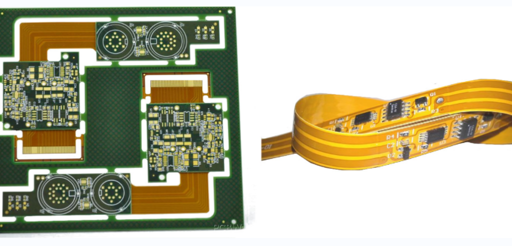
What is a Semi Rigid Flex PCB?
Definition
A semi rigid flex PCB is a type of printed circuit board that combines the benefits of both rigid and flexible PCBs. It consists of a combination of flexible and rigid substrates that are laminated together to form a single board. The flexible part of the board allows it to bend and twist, while the rigid part provides support and stability.
Advantages
Semi rigid flex PCBs offer several advantages over traditional rigid or flexible PCBs. These include:
- Space-saving: Semi rigid flex PCBs can be designed to fit into tight spaces, making them ideal for small electronic devices.
- Improved reliability: The combination of flexible and rigid substrates reduces the risk of damage to the board due to mechanical stress or vibration.
- Reduced assembly time: Semi rigid flex PCBs can be assembled more quickly than traditional PCBs, as they require fewer components and less wiring.
- Increased design flexibility: The flexibility of the board allows for more complex and innovative designs.
Applications
Semi rigid flex PCBs are used in a variety of applications, including:
- Aerospace and defense: The reliability and space-saving benefits of semi rigid flex PCBs make them ideal for use in aerospace and defense applications, such as avionics and radar systems.
- Medical devices: The flexibility and durability of semi rigid flex PCBs make them well-suited for use in medical devices, such as pacemakers and implantable sensors.
- Consumer electronics: Semi rigid flex PCBs are commonly used in consumer electronics, such as smartphones, tablets, and wearable devices.
Overall, semi rigid flex PCBs offer a unique combination of flexibility, durability, and space-saving benefits that make them an attractive option for a wide range of applications.
Design Considerations
When designing a semi rigid flex PCB, there are several important considerations to keep in mind. These include layer stackup, bend radius, material selection, trace width, and spacing.
Layer Stackup
The layer stackup of a semi rigid flex PCB is critical to its performance and functionality. It’s important to ensure that the layers are arranged in a way that provides the necessary mechanical and electrical properties. Typically, the stackup will consist of a combination of rigid and flexible layers, with the flexible layers providing the necessary flexibility for bending and folding.
Bend Radius
The bend radius of a semi rigid flex PCB is another important consideration. The bend radius determines how much the PCB can be bent before it experiences damage or failure. It’s important to choose a bend radius that is appropriate for the intended application. A smaller bend radius may be necessary for applications where space is limited, while a larger bend radius may be necessary for applications where the PCB will be subjected to more extreme bending.
Material Selection
The choice of materials for a semi rigid flex PCB is also critical. The materials must be able to withstand the mechanical stresses of bending and folding, as well as the electrical stresses of the application. Common materials used in semi rigid flex PCBs include polyimide, FR-4, and copper.
Trace Width and Spacing
The trace width and spacing of a semi rigid flex PCB are important considerations for ensuring proper electrical performance. The width and spacing of the traces must be chosen based on the electrical requirements of the application, as well as the mechanical constraints of the design. It’s also important to ensure that the traces are properly shielded and grounded to prevent interference and noise.
In summary, designing a semi rigid flex PCB requires careful consideration of several important factors, including layer stackup, bend radius, material selection, trace width, and spacing. By taking these factors into account, designers can create a PCB that meets the electrical and mechanical requirements of the application.
Manufacturing Process
Lamination
Semi-rigid flex PCBs are manufactured using a combination of rigid and flexible PCB materials. During the lamination process, the layers of the PCB are stacked and pressed together using heat and pressure. The rigid layers are typically made of FR4 or other similar materials, while the flexible layers are made of polyimide or similar materials. The number of layers in a semi-rigid flex PCB can vary depending on the application, but typically ranges from two to six layers.
Drilling
After lamination, the PCB is drilled to create the necessary holes for components and vias. The drilling process is critical to the success of the PCB, as any misalignment or damage to the holes can cause issues with the electrical connections. The drilling process is typically done using computer-controlled machines to ensure accuracy and consistency.
Plating
Once the holes have been drilled, the PCB is plated with copper to create the necessary electrical connections. The plating process involves applying a thin layer of copper to the surface of the PCB using a chemical process. The copper is then etched away in areas where it is not needed, leaving behind the necessary electrical connections.
Etching
The final step in the manufacturing process is etching. During this process, the excess copper is removed from the PCB to create the necessary electrical pathways. The etching process is typically done using a chemical solution that dissolves the excess copper. Once the etching is complete, the PCB is cleaned and inspected to ensure that it meets the necessary specifications.
Overall, the manufacturing process for semi-rigid flex PCBs is complex and requires a high degree of precision and expertise. However, by following the proper procedures and using the right materials and equipment, it is possible to create high-quality PCBs that meet the needs of a wide range of applications.
Testing and Inspection
Visual Inspection
Before beginning any testing, a visual inspection of the semi rigid flex PCB should be conducted. This inspection should be done to ensure that there are no visible defects, such as cracks, scratches, or other physical damage. The inspection should also include an examination of the solder joints, vias, and other components to ensure that they are properly connected and aligned.
Electrical Testing
Electrical testing is an important step in the testing and inspection process for semi rigid flex PCBs. This testing should be done to ensure that all of the connections and components are functioning properly. One common method of electrical testing is to use a multimeter to check the resistance and continuity of the circuit.
Mechanical Testing
Mechanical testing is another important step in the testing and inspection process for semi rigid flex PCBs. This testing should be done to ensure that the PCB can withstand the stresses and strains of its intended application. One common method of mechanical testing is to subject the PCB to a series of bending and twisting tests to ensure that it can withstand the expected forces.
In conclusion, testing and inspection are critical steps in the manufacturing process of semi rigid flex PCBs. Visual inspection, electrical testing, and mechanical testing are all important aspects of this process, and should be conducted with care and attention to detail to ensure that the PCB will function properly in its intended application.
Conclusion
In conclusion, semi rigid flex PCBs offer a unique solution for electronic devices that require both flexibility and rigidity. They are ideal for applications where space is limited and weight is a concern.
One of the key advantages of semi rigid flex PCBs is their ability to provide high-density interconnects in a compact package. This is achieved by combining the benefits of both rigid and flexible PCBs in a single design.

Additionally, semi rigid flex PCBs offer improved reliability compared to traditional rigid PCBs. This is due to the reduced number of interconnects and the elimination of connectors, which can be a source of failure in electronic devices.
Furthermore, semi rigid flex PCBs can be customized to fit the specific requirements of a particular application. They can be designed to include a variety of features, such as blind and buried vias, controlled impedance, and more.
Overall, semi rigid flex PCBs offer a versatile and reliable solution for a wide range of electronic devices. Their unique combination of flexibility and rigidity makes them an excellent choice for applications where space and weight are critical factors.
Comments are closed