Printed circuit board (PCB) vias are an essential component of modern electronics. These tiny holes, filled with conductive material, allow electrical signals to pass between layers of a PCB. Without vias, it would be impossible to create complex, multi-layered circuit boards that are critical to the functioning of everything from smartphones to spacecraft.
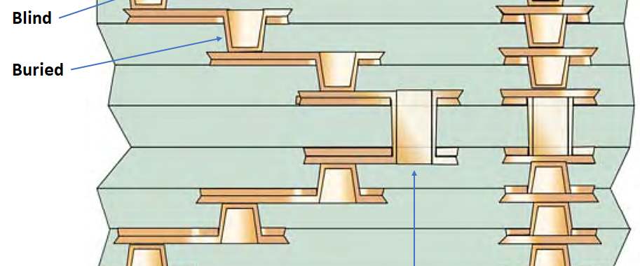
There are two main types of PCB vias: through-hole vias and blind/buried vias. Through-hole vias extend all the way through a PCB, connecting all layers. Blind vias connect an outer layer to an inner layer, while buried vias connect two inner layers. The choice of via type depends on the specific requirements of the circuit design, such as the number of layers, signal frequency, and board thickness.
The design and manufacturing of PCB vias has evolved significantly over the years, with advances in materials, drilling technology, and plating techniques. Today, PCBs can have hundreds of thousands of vias, each with precise dimensions and placement. The ability to create smaller and more complex vias has enabled the development of increasingly sophisticated electronics, paving the way for new applications and innovations.
What is a Printed Circuit Board Via?
Definition of a Via
A printed circuit board (PCB) via is a tiny hole that connects different layers of a PCB. It is used to transfer signals and power between different layers of the board. Vias are an essential component of multi-layer PCBs, which are used in complex electronic devices.
Types of Vias
There are several types of vias used in PCBs:
- Through-hole via: This type of via goes through the entire board, connecting all the layers. It is the most common type of via used in PCBs.
- Blind via: This type of via connects an outer layer of the board to an inner layer, but does not go through the entire board.
- Buried via: This type of via connects two inner layers of the board, but does not go through the entire board.
The choice of via type depends on the specific requirements of the PCB design.
In conclusion, a printed circuit board via is a crucial component of multi-layer PCBs that enables the transfer of signals and power between different layers of the board. There are different types of vias used in PCBs, each with its specific purpose.
Why are Vias Important in PCB Design?
Signal Integrity
Vias are crucial in maintaining signal integrity in PCB design. They allow for the transfer of signals between different layers of the board, ensuring that the signal remains strong and clear. Without vias, signals would have to travel longer distances, leading to signal loss and degradation. Vias also help reduce electromagnetic interference (EMI) by providing a direct path for signals to travel.
Thermal Management
Vias play a key role in thermal management in PCB design. They allow for the transfer of heat between different layers of the board, helping to dissipate heat and prevent overheating. Vias can also be used to connect thermal pads to ground planes, which helps to distribute heat evenly across the board.
Cost and Space Savings
Vias can help reduce the cost and space requirements of a PCB design. By allowing signals to travel between layers, vias can reduce the number of layers required in a board, which can lower the cost of manufacturing. Vias can also help reduce the size of a board by allowing components to be placed on both sides of the board, which can help save space.
In summary, vias are crucial in maintaining signal integrity, thermal management, and cost and space savings in PCB design.
How are Vias Manufactured?
Drilling Process
The first step in manufacturing vias is drilling holes in the printed circuit board (PCB). The holes are drilled using a high-speed drilling machine, which can drill through multiple layers of the PCB at once. The drilling process is critical because it determines the size and shape of the via.
To ensure accuracy, the drilling machine is programmed with the exact location and size of each via. The drill bits used in the process are made of tungsten carbide, which is a hard and durable material that can withstand the high speeds and pressures of the drilling process.
Plating Process
Once the holes have been drilled, the next step is the plating process. This involves depositing a thin layer of metal, typically copper, onto the walls of the holes. The plating process is essential because it creates a conductive pathway between the different layers of the PCB.
The plating process involves several steps, including cleaning the holes to remove any debris or contaminants, activating the holes to promote adhesion, and then electroplating the copper onto the walls of the holes. The thickness of the copper layer can be controlled to ensure that it is sufficient for the intended application.
After the plating process is complete, the PCB is cleaned again to remove any excess copper or other contaminants. The vias are now ready for use in the PCB.
Overall, the manufacturing process for vias is a precise and complex process that requires specialized equipment and skilled technicians. However, with the proper equipment and expertise, high-quality vias can be produced consistently and reliably.
Common Issues with PCB Vias
Via-in-Pad
Via-in-pad is a technique used to reduce the size of PCBs. It involves placing vias directly under surface-mount components. While this technique can save space, it can also cause issues such as solder bridging and uneven heating during reflow. This can result in poor electrical connections and damage to components.
Stub Vias
Stub vias are vias that do not pass through the entire board. They can cause signal reflection and interference, leading to poor signal quality. Stub vias can also cause impedance mismatches, resulting in signal loss and distortion.

Tenting and Filling
Tenting and filling refer to the process of covering or filling vias with a material such as solder mask or epoxy. While this can protect the vias from environmental damage, it can also cause issues such as trapped air, which can lead to voids and poor connections. Tenting and filling can also increase the cost of PCB production.
In addition to these issues, other common problems with PCB vias include misaligned or broken vias, plating issues, and thermal expansion. It is important to carefully design and test PCBs to ensure the vias function properly and do not cause any issues.
Overall, PCB vias are an important component of electronic devices, but they can also cause issues if not designed and implemented properly. By understanding these common issues and taking steps to address them, designers can create reliable and high-quality PCBs.
Conclusion
Printed circuit board (PCB) vias are an essential component in the design and manufacture of modern electronic devices. They provide a means of connecting different layers of a PCB, allowing for the routing of signals and power between components.
There are various types of vias available, each with its own advantages and disadvantages. Through-hole vias are commonly used for high-current applications, while blind and buried vias are ideal for high-density designs. Microvias are used for fine-pitch devices, and back-drilled vias are used to reduce signal reflections.
When designing a PCB, it is important to consider the size, shape, and placement of vias carefully. This can have a significant impact on the performance, reliability, and cost of the final product.
In summary, PCB vias are a critical part of modern electronics, and their design and implementation require careful consideration. By understanding the different types of vias available and their respective benefits, designers can create more efficient and reliable PCBs that meet the needs of today’s demanding applications.
Comments are closed