Heavy copper PCBs are becoming increasingly popular in the electronics industry due to their ability to handle high currents and withstand extreme temperatures. These PCBs are designed with thicker copper layers than standard PCBs, making them ideal for applications that require high power and reliability. Heavy copper PCBs are commonly used in power supplies, automotive electronics, and industrial equipment.
One of the main advantages of heavy copper PCBs is their ability to handle high currents. The thicker copper layers allow for better heat dissipation and lower resistance, reducing the risk of overheating and voltage drops. This makes heavy copper PCBs ideal for applications that require high power, such as electric vehicles and renewable energy systems. Additionally, heavy copper PCBs can withstand extreme temperatures, making them suitable for use in harsh environments.
Designing heavy copper PCBs requires specialized knowledge and expertise. The increased thickness of the copper layers can affect the overall design of the PCB, and the use of heavy copper requires careful consideration of the manufacturing process. However, with proper design and manufacturing techniques, heavy copper PCBs can provide superior performance and reliability compared to standard PCBs.
What is Heavy Copper PCB Design?
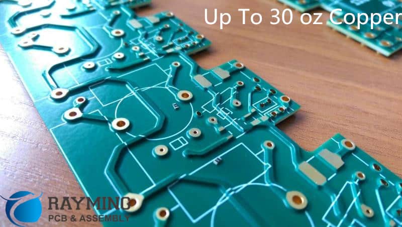
Heavy copper PCB design refers to the process of manufacturing printed circuit boards with thicker copper layers than standard PCBs. Generally, copper layers with a thickness of 3 oz/ft² or more are considered heavy copper PCBs.
The heavy copper PCB design has become increasingly popular due to its ability to handle high currents and increase the overall reliability of the PCB. The increased copper thickness of heavy copper PCBs also provides better thermal management, which makes them ideal for applications that generate a lot of heat.
Heavy copper PCBs are commonly used in power electronics, automotive, and aerospace industries, where high power and reliability are critical. They are also used in applications that require high current carrying capacity, such as power supplies, motor controllers, and battery management systems.
In addition to their superior electrical and thermal properties, heavy copper PCBs offer several other benefits. They provide better mechanical strength, which makes them more resistant to bending and warping. They also have a longer lifespan than standard PCBs, which makes them ideal for applications that require long-term reliability.
Overall, heavy copper PCB design is an excellent choice for applications that require high power, high current, and reliable performance.
Advantages of Heavy Copper PCB Design
Increased Durability
Heavy copper PCBs are designed to withstand high current and voltage levels. They have thicker copper traces and larger vias, which make them more durable than standard PCBs. This makes them ideal for use in applications that require high reliability and long-term durability.
Improved Thermal Management
Heavy copper PCBs have a higher thermal conductivity than standard PCBs. This means that they can dissipate heat more efficiently, which is important for applications that generate a lot of heat. They are also less likely to experience thermal stress, which can cause damage to the PCB and its components.
Better Electrical Performance
Heavy copper PCBs have a lower impedance and better signal integrity than standard PCBs. This is because the thicker copper traces reduce the resistance of the traces, which in turn reduces the impedance. This makes them ideal for use in high-speed digital circuits, RF circuits, and power electronics.
In summary, heavy copper PCBs offer several advantages over standard PCBs, including increased durability, improved thermal management, and better electrical performance. These advantages make them ideal for use in a wide range of applications, from automotive and aerospace to medical and industrial.
Design Considerations for Heavy Copper PCBs
When designing heavy copper PCBs, there are a few important design considerations to keep in mind to ensure the reliability and performance of the board. In this section, we will discuss three key design considerations: trace width and spacing, via size and placement, and drill size and tolerance.
Trace Width and Spacing
The trace width and spacing on a heavy copper PCB are critical factors that affect the board’s performance. To ensure the proper current carrying capacity, the trace width should be increased to accommodate the higher current density. The spacing between traces should be increased to prevent arcing and ensure proper insulation.
Via Size and Placement
Vias are an essential component of a heavy copper PCB, as they provide a path for current to flow through the board. The size and placement of vias are crucial in ensuring the proper functioning of the board. The via size should be increased to accommodate the higher current density, and the number of vias should be increased to ensure proper heat dissipation.
Drill Size and Tolerance
The drill size and tolerance are critical factors that affect the reliability of the board. The drill size should be increased to accommodate the larger copper layers, and the tolerance should be tightened to ensure proper alignment of the layers. It is also recommended to use a laser drill for better accuracy and precision.
In summary, designing a heavy copper PCB requires careful consideration of trace width and spacing, via size and placement, and drill size and tolerance. By keeping these factors in mind, you can ensure the reliability and performance of your board.
Manufacturing Process for Heavy Copper PCBs
Lamination Process
The first step in manufacturing heavy copper PCBs is the lamination process. It involves the stacking of multiple layers of copper and substrate materials. The layers are then pressed together using heat and pressure to form a single, solid board.
The final thickness of the board is determined by the number of layers used. The lamination process is crucial to the overall quality of the heavy copper PCB, as it ensures that the layers are properly bonded and that there are no air pockets or voids between them.
Copper Plating Process
Once the board is laminated, the next step is the copper plating process. This involves the deposition of copper onto the surface of the board, which is then used to create the circuitry.
The copper plating process is typically done using an electroplating method, where a layer of copper is deposited onto the surface of the board using an electric current. This process is repeated until the desired copper thickness is achieved.
Etching Process
The final step in the manufacturing process for heavy copper PCBs is the etching process. This involves the removal of unwanted copper from the surface of the board to create the circuitry.
The etching process is typically done using a chemical solution, which is applied to the surface of the board. The solution dissolves the unwanted copper, leaving behind the desired circuitry.
Overall, the manufacturing process for heavy copper PCBs requires precision and attention to detail at every step. By following these steps carefully, manufacturers can ensure that their heavy copper PCBs are of the highest quality and meet the needs of their customers.
Applications of Heavy Copper PCBs
Heavy copper PCBs are widely used in various industries due to their ability to withstand high currents and high temperatures. The following are some of the most common applications of heavy copper PCBs:

Power Electronics
Heavy copper PCBs are commonly used in power electronics such as power supplies, inverters, and converters. These applications require high current carrying capacity and low impedance, which can be achieved by using thick copper layers. Heavy copper PCBs also offer better thermal management, which is essential in power electronics.
Automotive Electronics
Automotive electronics require high reliability and durability due to the harsh environment they operate in. Heavy copper PCBs are ideal for automotive electronics due to their ability to withstand high temperatures, vibrations, and moisture. They are commonly used in engine control units, transmission control units, and other critical systems.
Aerospace and Defense
Aerospace and defense applications require high-performance PCBs that can withstand extreme temperatures, vibrations, and shock. Heavy copper PCBs are commonly used in avionics, satellite systems, and military equipment. They offer high reliability and durability, which is essential in these applications.
In summary, heavy copper PCBs offer a range of benefits that make them suitable for various applications. They provide high current carrying capacity, low impedance, and better thermal management, which is essential in power electronics. They also offer high reliability and durability, making them ideal for automotive electronics, aerospace, and defense applications.
Comments are closed