Since Printed Circuit Boards (PCBs) came to beckon a standard in the manufacturing of electrical and electronic appliances, there has been some competition of sorts among the boards.
Ideally, there are different types of PCBs, which makes it competitive as one board type tries to hold the upper hand over the others. Besides, the trio of the Single-Sided PCB, the Double-Sided PCB, and the Multilayer PCB are commonly used.
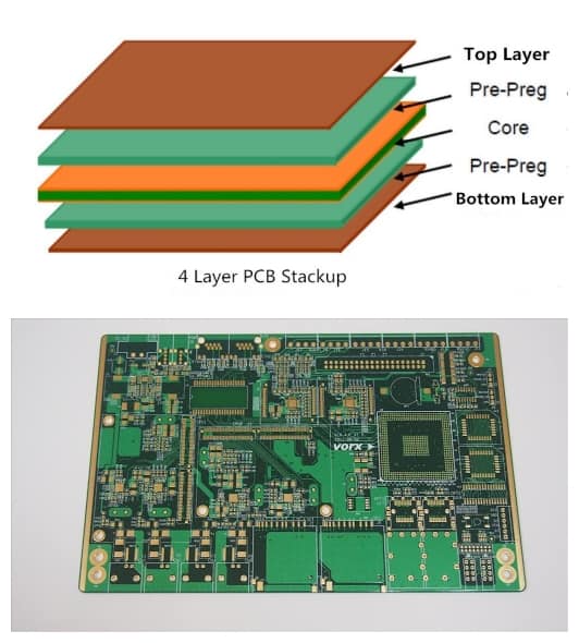
The 4 Layer PCB
Now, the 4 Layer PCB, which happens to fall under the Multilayer PCB, has been in the spotlight for some time. This is in consideration of the fact that it has some amazing properties that have been causing PCB customers and buyers to think of getting one of it.
In this article, we shall take you on a tour of the important things you need to know about the 4 Layer PCB. You will discover why it has the upper hand instead of its competitor – the 2 Layer PCB.
Besides, the massive use of the 4 Layer PCB and the various use cases combine to make it one of the Printed Circuit Boards (PCBs) that cannot be ignored.
————————————————————-
Request 4Layer PCB Manufacturing & Assembly Quote, Pls Send PCB File to Sales@raypcb.com Now
————————————————————-
Is 4 Layer PCB Complex?
The designing and the manufacturing of Printed Circuit Boards (PCBs) doesn’t come easy. You will have to be patient throughout the process. You will also need to pay attention to the procedure so you don’t miss anything.
Also, you have to understand the complexity of the Printed Circuit Boards (PCBs) tend to vary by the types. The complexity or difficulty experienced with the designing and the manufacturing of the Single-Sided PCB is not the same as the 4 Layer PCB. It is because the complex nature of the 4 Layer PCB is higher than the others are.
So, the 4 Layer PCB is quite complex because it falls under the category of the Multilayer PCBs.
We will also like to point out that the Multilayer Printed Circuit Boards (PCBs) are not limited to the 4 Layer PCB alone. Instead, they can go as high as eight layers. In the light of that, every other increment in the layers attracts the addition or integration of two more layers to the board.
Dissecting the 4 Layer PCB
The components of the 4 Layer PCB must be dissected. Here, we will look at the different layers that make up the 4 Layer PCB.
- Top Layer
The four (4) layers that make up the 4 Layer PCB are divided into three categories. The Top Layer is the first category.
As the name suggests, the Top Layer is placed at the top part or section of the board. The Top Layer is also part of the outer layers (including the Bottom Layers). These outer layers form the sections for the placement of components and routing.
Aside from the Top Layer, there are other important layers, which are placed beneath it. These are not part of the other layers that make it four (4).
The first layer, in this case, is the Signal Layer, which has a width of about 0.0014 inches.
The second layer that comes after it is the Preg Layer. It has a dielectric constant of 4.2 and a thickness of about 0.0091 inches.
Generally, the components of the Top Layer are made of copper material. After the Top Layer, there are two other layers, which will be discussed below.
- The Core Layer
The next layer is the Core Layer. It is called the Core Layer because it has most of the important components that power the Printed Circuit Board (PCB).
The Core Layer in this instance refers to the Inner Layer 1 and the Inner Layer 2. These layers (Inner Layer 1 and Inner Layer 2) are often used for signal routing and as power planes.
To break them down further, we will look at the individual parts or components of each of the aforementioned layers.
On the one hand, there is Inner Layer 1. Here, there is the Pre-Preg Layer, which is generally called the Plane. It is closely followed by the Inner Layer 1 of 0.0014 inches. There is also the Core Sublayer, which is a part of the Inner Layer 1. The Core Sublayer has a width of about 0.0037 inches.
On the other hand, there is the Inner Layer 2, which forms part of the Core Layers for the 4 Layer PCB. It has a Plane Layer that comprises a thickness of 0.0014 inches. The Plane Layer also has 1 oz. of copper. The Inner Layer 2 also has a Pre-Preg Layer that has two sheets of thickness 0.0091 inches.
- Bottom Layer
The Bottom Layer is the last layer or part of the 4 Layer PCB. It also doubles as a Signal Layer (just like the Top Layer is) and has a thickness of 0.0014 inches.
————————————————————-
Request 4Layer PCB Manufacturing & Assembly Quote, Pls Send PCB File to Sales@raypcb.com Now
————————————————————-
How to Design the 4 Layer PCB Stack Up
If you are looking at how to design the stack up for the 4 Layer PCB, we got you covered.
We are presenting you with three options.
Option 1:
Under this option, the idea is to design the stack up using one layer of power supply, two signal layers, and one ground layer.
Here are itemized steps to achieve that:
- The Top Layer (the Power Layer) comes first
- The Signal Layer (Layer 2) comes next
- Layer 3 (the Signal Layer too) follows
- The Ground Layer (the Bottom Layer) comes last
This design aims to achieve a specific shielding effect by placing the power and the ground layers at the top and the bottom layers of the 4 Layer PCB, respectively.
Option 2:
If you don’t want to use the first option (as discussed above), you want to use the second option instead.
The second option we have here is designed to decouple the effect of the power plane/layer. It can also contribute to the reduction of the distributed impedance of the ground layer and the top layer, only if the impedance control board is not too thick.
Here is how to design the stack-up of the 4 Layer PCB using the second option we just discussed:
- The Top (Signal Layer) comes first
- The Ground Layer (Layer 2) comes next
- The Power Layer (Layer 3) follows
- The Signal Layer (the Bottom Layer) is the last
Option 3:
There is the third and last option you can leverage to design the stack-up of the 4 Layer PCB.
This option is usually used when there is a need to wire the underlying signal layer or the bottom layer.
Here is how to design the 4 Layer PCB stack up using the third option:
- The Signal Layer (the Top Layer) comes first
- The Power Layer (Layer 2) follows
- The Ground Layer (Layer 3) comes under Layer 2
- The Signal Layer (the Bottom Layer) will be the last
————————————————————-
Request 4Layer PCB Manufacturing & Assembly Quote, Pls Send PCB File to Sales@raypcb.com Now
————————————————————-
Important Aspects of the 4 Layer PCB
The 4 Layer PCB has specific features that set it apart from the other Printed Circuit Boards (PCBs).
Here are some of them:
- Altering the Layers
The layers of the 4 Layer PCB can be altered without any glitches. This makes it better than the other types of PCBs, which may develop some issues when the layers are altered.
The focus is on the altering of the layers, which are connected by vias. The vias, which are plated holes that pass through the substrate to connect different layers of the copper, plays an important role in the 4 Layer PCB.
The vias of the 4 Layer PCB can be altered in many ways. Some of them are:
- Burying the vias in the PCB in a way that it still connects the internal layers while “out of sight.”
- There is also the option to run the vias as “through vias,” meaning that it can connect all the layers.
- The vias can also be used in a “blind vias” format whereby it runs to some length and stops the connection at a specific point in the Printed Circuit Board.
- More Surface Area Tracing
More surface areas can be traced in the 4 Layer PCB. This is bolstered by the use of the Pre-Preg layer that provides dielectric between the layers.
It is also because of the application of heat and pressure using the Pre-Preg layer. This, in turn, helps to bond the Single-Sided PCBs and the Multilayer PCBs.
- Higher Sensitivity
The 4 Layer PCB has a higher sensitivity more than the other types of Printed Circuit Boards (PCBs). It also reduces propagation levels, uses a complex design, and reduces distortion.
Final Thoughts
When you are looking at making use of the 4 Layer PCB for your next Printed Circuit Boards (PCBs), make sure you have understood the things that are involved.
Above all, ensure that you contact a reliable PCB manufacturer that offers instant quotes, the best materials, and affordable pricing.
So, what do you think of the 4 Layer PCB?
Comments are closed