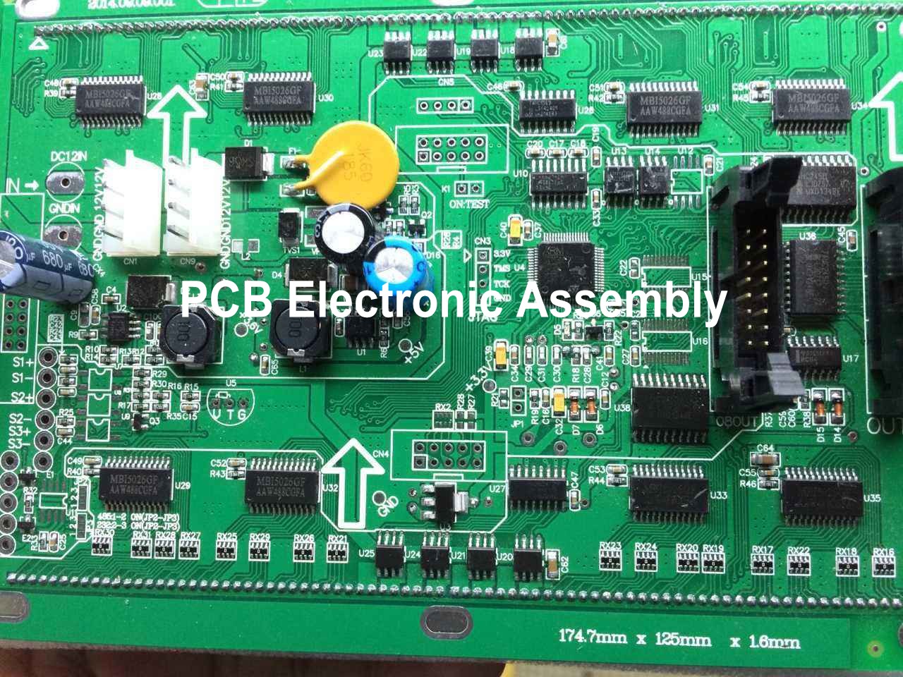
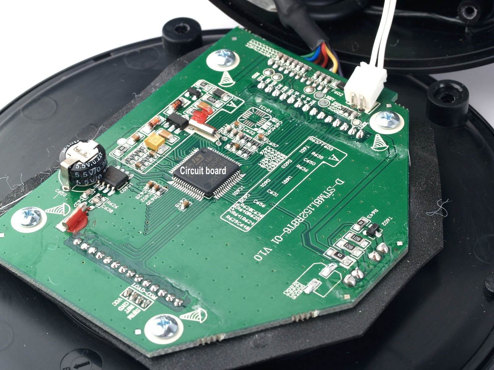
PCB Assembly:How Electronic Components are Assembled on PCBs 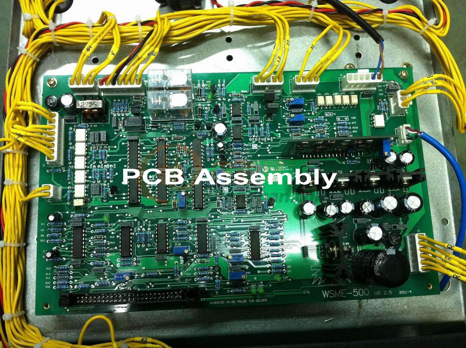
Printed circuit boards (PCBs) are now an integral part of everyday life across various industries, including Industrial, Medical, Automotive, Rail, Marine, and Security electronics. There are multiple aspects of electronic assembly such as the assembling of flexible PCB circuits, using thermal substrates for boards, producing PCBs with blind and buried vias, quality of the electronic components, selecting manufacturers and distributors for the parts, storage of moisture and temperature-sensitive components, and using different assembling technologies such as through-hole and surface-mount technology.
Modern PCB assembly facilities are equipped with state-of-the-art machines and incorporate both surface-mount and through-hole assembling technologies. These facilities offer different service levels – from supplying PCB prototypes to the manufacturing of complex, multi-technology printed circuit boards. Characteristics of contemporary electronic assembly include automatic pick and place lines for SMT devices, Conventional assembly by hand, automated optical inspection, lead-free wave soldering, ICT and ATE electrical tests, conformal coating, and potting and encapsulation.
There are various methods for assembling electronics, and every supplier has a specialized process. In this article, we have compiled some of the steps of the printed circuit board assembly. Only once the model has been validated, prototyped, and checked will PCB assembly begin. Usually, an electronic assembly comprises of the following stages:
- Stenciling for Applying Solder Paste on PCBs.
- Selection and Placement of Components.
- Reflow Soldering.
- Manual Soldering of PTH devices.
- Inspection and Testing of PCBs.
- Washing of PCBs.
- Packaging of Assembled Boards.
————————————————————-
Request Electronic Contract Manufacturing Quote, Pls Send PCB File to Sales@raypcb.com Now
————————————————————-
Stenciling for Applying Solder Paste on PCBs
Solder paste stenciling is similar to the silkscreen stenciling technique. In silkscreen stenciling, a mask is laid over the surface where you want to apply the ink, whereas, in solder paste stenciling, a template stencil is used for the application of the paste to particular areas of a PCB. The stencil process starts with either a single PCB or a bigger PCB, with the circuit patterned several times to make the process a little faster. On each pad where a part is put, a small dab of solder paste is added. The stencil is placed over the board for smaller-scale assembly, and the paste with a metal squeegee is spread over the stencil.
A solder paste is typically a metal alloy combing different percentages of tin, copper, and silver. Pastes generally have an expiry date and are needed to be kept in a specific temperature range. Flux may lose its strength if stored n unfavorable conditions. Flux alters the metal’s surface friction as it is in a liquid state, helping it move through the joints. Solder paste is available in two types, one is lead-free solder paste, and another is leaded solder paste. Electronics circuit boards supplied to Europe must use lead-free solder paste due to European Union rules and regulations. Otherwise, the leaded paste is more flexible and more comfortable to use.
Different computer applications are used to design PCBs, such as Altium Designer, Autodesk Eagle, and Dip Trace. The program generates several layer files used by the PCB maker to generate the final PCB. Two layers are essential for making stencils: the top paste layer and the bottom paste layer. A stencil fabricator uses these two layers to carve out the stencils from thin sheets of stainless steel through a high-power CO2 laser.
Stenciling can also be done by hand if the PCB assembly is carried out on a smaller scale. The stencil is carefully lined up over the board by hand in the manual method, and then solder paste is applied. The paste is applied evenly onto a stencil using metal scrapers such as putty knives. There are automatic stenciling machines. These machines are very complex pieces of equipment, but they make stenciling a lot easier in large production runs.
Selection and Placement of Components
The components are mounted over the PCB after the paste was added to the board. The paste helps temporarily secure the components on the board. The component placement can be achieved either by hand or by a machine. One way to manually place components is by using tweezers. You Pick the component up using a tweezer and place it one by one on the board. Placing components by hand is an entirely accurate process because, during reflow, the liquid solder can move the parts to their correct place due to its surface tension. But, on an industrial scale, working manually is not plausible. It gets harder to position components after a couple of hours easily. And the placement of small-sized SMT devices quickly becomes challenging. On an industrial scale, this process is handled by large machines. These machines are called pick and place (PNP) machines. They are especially useful for placing SMT components PNP unit is a robotic assembly platform that selects a component using a vacuum, rotates it to the proper position, and then places it on a PCB. Setting up a computer to build the assembly takes a few hours, but it is efficient once it works. PNP machines can build hundreds of boards in a lot less time. In industrial-scale warehouses, a conveyor belt carries the board from an automatic paste applying system through the PNP machines.
————————————————————-
Request Electronic Contract Manufacturing Quote, Pls Send PCB File to Sales@raypcb.com Now
————————————————————-
Reflow Soldering
It is crucial to reflow the paste after pick-and-place to build a stable connection. The PCBs are mounted on a conveyor belt passing steadily inside an oven, heating the boards adequately at about 250 °C to melt the solder. It experiences multiple temperature zones as the board passes through the oven, enabling it to warm up and cool down at a regulated pace. The paste is like sticky glue. Although the board steadily travels through the reflow oven, the pieces remain in place. The reflow device is sort of like a baking oven. The board’s temperature is raised to around 250 °C (480 °F), at which point the paste turns into liquid metal. When the board leaves the reflow oven, it quickly cools, soldering all of the components in order. There are various stages of reflow soldering. There are small grey blobs of solder paste on the different pads in the beginning. Then the flux becomes runnier inside the paste and starts to produce droplets.
Initially, the solder is in solid form, Then the solder begins to melt, and the melting solder’s surface friction allows the melting solder to leave droplets of solder on pads of PCB In reflow, the solder can move the parts to some extent. Some components end up entirely out of place and require manual adjustment later. The solder tends to push and pull components slightly. This phenomenon is beneficial during reflow because the small misalignments are corrected without any interventions. Conversely, if one end of the component is pulled faster than the other, with very tiny bits, the effect, called tombstoning, may cause a part to stand on one leg. It leads the board to have a functional flaw. Finally, the board comes out of the oven, and it is cooled down, the solder solidifies, and the components are fully soldered to the PCB.
Reflow Soldering for two-sided PCBs
In various assemblies, electronic parts are located on two sides of the PCB. In these cases, the sheet with the least and shortest components is first stenciled and reflowed. It is stenciled and reflowed once more on the other side when the PCB comes out of the oven after reflow. The metal’s surface tension is extreme and keeps everything in place. During the pick and place process in larger plants, different parts of the board may be glued to ensure that the components do not shift their location during reflow, especially in more complicated assemblies.
Manual Soldering of PTH devices
After reflow, any plated through-hole (PTH) parts are manually picked up by a technician and soldered to the board by hand. Using a wave soldering procedure in the broader production facility, where the board is passed over a standing wave of liquid solder that clings to part leads and any visible metal on the PCB, the soldering of through-hole parts may be accomplished. However, SMD (surface mount devices) have become an industry standard. The use of the PTH component has become limited; therefore, small and medium-range facilities prefer to hand solder any PTH components
Inspection and Testing of PCBs
The next step in the assembly of PCBs is optical checking. The optical inspection identifies issues with the components such as the wrong resistor, missing capacitor, and short circuits. The automated optical inspection (AOI) machine works very fast, almost in real-time. The AOI requires various high-power cameras at various angles to see different aspects of the solder joints or fillets. Light is reflected differently from poorly soldered fillets compared to an adequately soldered one; therefore, the AOI uses different colored LEDs to illuminate and examine any link, with great precision and at a very high pace. Optical inspection checks ensure all of the correct components are on the board, in the right places, with correct solder fillets and no short circuits caused by extra solder between adjacent pins. After the inspection, the board is prepared for testing to ensure it does what it is supposed to do.
Testing takes a lot of time. In extensive assembling facilities, thousands of boards are made every day. To speed up the testing process, automatic test fixtures are used. Test fixtures are temporary electrical contacts used to verify the controllers’ voltage output, the predicted voltages on individual pins, and giving different orders to the test board to ensure that it reacts appropriately. More measures are taken to load code and validate the performance on boards that need programming or additional tuning.
More expansive facilities use a flying probe or advanced bed of nail fixtures to verify any board’s link for consistency before powering the board. For more sophisticated, pricey items, these larger fixtures are appropriate.
Washing of PCBs
Different processing stages leave residues on the PCBs Soldering leaves a slight amount of flux on the board regularly. This flux residue remains sticky with time and may turn slightly acidic, contributing to solder joints becoming damaged. To avoid the sticking of this residue, the PCBs are washed after the initial assembling process. The boards are cleaned using a machine similar to a dishwasher. This high temperature, high speed, and all stainless-steel dishwasher utilize deionized water to eliminate all contamination from the development stages. A closed-loop scheme is used for the parts washer. After cleaning, the wastewater is stored in a separate container, and conductivity is automatically measured. The washing is assumed to be complete if its resistance is very high, then the wastewater is recycled through filters.
For DIY purposes, there is no need to uses expensive machines. The critical ingredient for cleaning electronics is using deionized water. Deionized water is ion-free water. Instead, the water does not kill the circuitry; it is the ions that cause various tiny parts of the device to provide electricity. It is very harmful to humans to drink because DI water does not contain ions. Although it’s OK to handle DI water, consuming, as it allows your body to lose ions quickly, DI water can do considerable damage to your body. Since DI water readily absorbs ions, the interior of the dishwasher is entirely made of stainless steel. Every other metal will disintegrate rapidly. A cotton swab or a brush with any isopropyl alcohol can also perform very well with just a handful of PCBs. A fan or compressed air is useful for extracting any leftover water.
Packaging of Assembled Boards
The packaging is the final stage of the electronic circuit board assembly. When the PCB batch is clean and dry, it will be wrapped up, where every PCB is thermally sealed into ESD plastic individually. Picking and packing orders ought to be as quick as possible in a broad industrial environment. Most of the products are labeled using barcodes for easy identification. The product name, SKU, and a batch ID are included in the bar code label to track problems. When the PCB has been thoroughly assembled, it is forwarded to the shipment floor for distribution.
Comments are closed