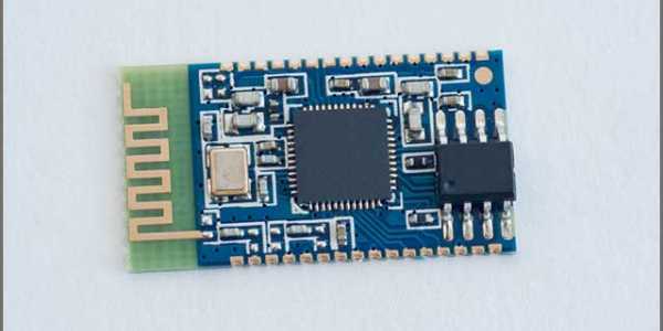
Bluetooth PCB design is an essential aspect of modern electronic devices. It involves designing printed circuit boards that enable wireless communication using Bluetooth technology. These circuit boards are used in a wide range of devices, including smartphones, laptops, and wearable devices.
Designing a Bluetooth PCB involves several critical considerations, such as antenna placement, power consumption, and data transfer rates. The placement of the antenna is particularly crucial, as it can greatly affect the signal strength and range of the Bluetooth connection. Power consumption is another important factor, as Bluetooth devices are often powered by batteries, and optimizing power usage can extend the device’s battery life. Additionally, data transfer rates must be carefully considered to ensure that the device can transfer data quickly and efficiently.
Overall, designing a Bluetooth PCB requires a thorough understanding of the technology and the specific requirements of the device. With the increasing popularity of Bluetooth-enabled devices, the demand for skilled PCB designers is also on the rise. As a result, it is essential for electronics engineers and designers to have a solid understanding of Bluetooth PCB design principles to create high-quality, efficient devices.
Understanding Bluetooth PCB Design
What is Bluetooth PCB Design?
Bluetooth PCB design is the process of designing printed circuit boards that allow Bluetooth-enabled devices to communicate wirelessly. PCB design involves creating a layout that includes the necessary components, such as antennas, transceivers, and microcontrollers, and arranging them in a way that optimizes performance and minimizes interference.
Why is Bluetooth PCB Design Important?
Bluetooth PCB design is crucial for ensuring reliable and efficient wireless communication between devices. A well-designed PCB can improve the range and stability of the Bluetooth signal, reduce power consumption, and minimize the risk of interference from other electronic devices.
When designing a Bluetooth PCB, it is important to consider factors such as antenna placement, signal routing, and power management. Antennas should be positioned to maximize signal strength and minimize interference, while signal routing should be optimized to reduce noise and ensure reliable communication. Power management is also critical, as Bluetooth devices often operate on battery power and require efficient power usage to conserve energy.
Overall, effective Bluetooth PCB design is essential for creating high-quality, reliable Bluetooth-enabled devices that can communicate seamlessly with other devices. By carefully considering the layout and components of the PCB, designers can optimize performance, reduce interference, and ensure a smooth and reliable user experience.
Key Considerations for Bluetooth PCB Design
When designing a PCB for a Bluetooth device, there are several key considerations that must be taken into account. These considerations include antenna design, power consumption, noise reduction, signal integrity, RF layout, component placement, and routing.
Antenna Design
The antenna is a critical component of any Bluetooth device, as it is responsible for transmitting and receiving signals. The antenna must be designed to match the frequency of the Bluetooth signal and be placed in an optimal location on the PCB. The size and shape of the antenna should also be carefully considered to ensure maximum performance.
Power Consumption
Bluetooth devices are typically powered by batteries, so power consumption is an important consideration. The PCB should be designed to minimize power consumption by optimizing the use of low-power modes and reducing the number of components that require power.
Noise Reduction
Noise can interfere with the Bluetooth signal and reduce performance. The PCB should be designed to minimize noise by using proper grounding techniques and shielding sensitive components from noise sources.
Signal Integrity
Signal integrity is critical for the reliable transmission and reception of Bluetooth signals. The PCB should be designed to minimize signal loss and distortion by using proper trace routing techniques and ensuring that signal traces are kept away from noise sources.
RF Layout
The layout of the PCB can have a significant impact on the performance of the Bluetooth device. The RF layout should be carefully designed to minimize signal loss and interference by using proper trace routing techniques and ensuring that the antenna is placed in an optimal location.
Component Placement
The placement of components on the PCB can also impact the performance of the Bluetooth device. Components should be placed in a way that minimizes signal loss and interference, and that allows for optimal antenna placement.
Routing
Trace routing is critical for ensuring signal integrity and minimizing interference. The PCB should be designed with proper trace routing techniques in mind, including the use of differential signaling and avoiding sharp corners and right angles.
In summary, when designing a PCB for a Bluetooth device, there are several key considerations that must be taken into account. These considerations include antenna design, power consumption, noise reduction, signal integrity, RF layout, component placement, and routing. By carefully considering these factors, designers can ensure that their Bluetooth devices are reliable and perform optimally.
Tools and Techniques for Bluetooth PCB Design

Bluetooth PCB design requires the use of specific tools and techniques to ensure proper functionality and performance. This section will discuss the essential tools and techniques needed for Bluetooth PCB design.
PCB Design Software
PCB design software is crucial for creating a Bluetooth PCB design. It allows designers to create schematics, layout designs, and generate Gerber files for manufacturing. Some popular PCB design software for Bluetooth PCB design include:
- Altium Designer
- Eagle PCB Design
- KiCAD
- OrCAD
Each software has its strengths and weaknesses, and designers should choose the one that best suits their needs.
Simulation and Testing Tools
Simulation and testing tools are essential for ensuring the functionality and performance of a Bluetooth PCB design. These tools allow designers to simulate and test the design before manufacturing, reducing the risk of errors and costly mistakes. Some popular simulation and testing tools for Bluetooth PCB design include:
- LTSpice
- PSpice
- Multisim
- CircuitMaker
These tools allow designers to simulate the performance of the design, test for errors, and optimize the design for better performance.
Prototyping and Manufacturing
Prototyping and manufacturing are the final stages of Bluetooth PCB design. Prototyping allows designers to test the design in a real-world environment, while manufacturing allows for mass production of the design. Some popular prototyping and manufacturing tools for Bluetooth PCB design include:
- 3D printing
- CNC milling
- PCB assembly services
These tools allow designers to create prototypes and manufacture the design for mass production.
In conclusion, the tools and techniques used in Bluetooth PCB design are critical for ensuring proper functionality and performance. Designers should carefully choose the PCB design software, simulation and testing tools, and prototyping and manufacturing tools that best suit their needs.
Best Practices for Bluetooth PCB Design
When designing a Bluetooth PCB, there are several best practices that should be followed to ensure success. These practices include designing for manufacturability, testability, and reliability.
Design for Manufacturability
Designing for manufacturability means designing a PCB that can be easily and efficiently manufactured. This includes minimizing the number of components, reducing the number of layers, and ensuring that the design can be easily scaled for high-volume production.
To achieve this, designers should consider the following:
- Use surface mount components whenever possible
- Avoid complex routing
- Use standard component sizes and footprints
- Minimize the use of vias
- Use a single-sided PCB design if possible
By following these guidelines, designers can ensure that their Bluetooth PCBs can be manufactured quickly and efficiently.
Design for Testability
Designing for testability means designing a PCB that can be easily tested during the manufacturing process. This includes adding test points, using built-in self-test (BIST) circuits, and ensuring that the design can be easily debugged if issues arise.
To achieve this, designers should consider the following:
- Add test points to critical components and signals
- Use BIST circuits to test critical components
- Ensure that the design can be easily debugged using standard tools and methods
By designing for testability, designers can ensure that their Bluetooth PCBs can be tested quickly and efficiently during the manufacturing process.
Design for Reliability
Designing for reliability means designing a PCB that can withstand the rigors of everyday use. This includes ensuring that the design is robust, using high-quality components, and following best practices for thermal management.
To achieve this, designers should consider the following:
- Use high-quality components from reputable manufacturers
- Follow best practices for thermal management, including proper component placement and the use of heat sinks or other cooling methods
- Use conformal coating or other protective measures to prevent damage from moisture or other environmental factors
By designing for reliability, designers can ensure that their Bluetooth PCBs will perform well over time and provide a positive user experience.
In summary, by following best practices for manufacturability, testability, and reliability, designers can ensure that their Bluetooth PCBs are efficient, reliable, and easy to manufacture and test.
Challenges and Solutions for Bluetooth PCB Design
When designing a printed circuit board (PCB) for a Bluetooth device, there are several challenges that designers need to overcome to ensure the device operates correctly. This section will discuss some of the most common challenges and solutions for Bluetooth PCB design.
Interference and Coexistence
One of the biggest challenges for Bluetooth PCB design is interference and coexistence. Bluetooth operates in the 2.4 GHz frequency band, which is also used by other wireless technologies such as Wi-Fi and Zigbee. This can cause interference and coexistence issues, which can lead to reduced performance and reliability of the Bluetooth device.
To overcome these challenges, designers need to carefully design the PCB layout to minimize interference and ensure coexistence with other wireless technologies. This can be achieved by using techniques such as frequency hopping and channel selection, as well as optimizing the antenna design and placement.
EMI/EMC Compliance
Another challenge for Bluetooth PCB design is ensuring compliance with electromagnetic interference (EMI) and electromagnetic compatibility (EMC) regulations. Bluetooth devices can emit electromagnetic radiation, which can interfere with other electronic devices and cause compliance issues.
To ensure compliance with EMI/EMC regulations, designers need to carefully design the PCB layout and use shielding and filtering techniques to minimize electromagnetic radiation. This can include using ferrite beads, EMI filters, and shielding cans.
Cost Optimization
Finally, cost optimization is also a challenge for Bluetooth PCB design. Bluetooth devices often require multiple components, including microcontrollers, radio modules, and antennas, which can increase the cost of the device.
To optimize costs, designers need to carefully select components and use techniques such as integrating components and reducing the number of layers in the PCB. This can help to reduce the overall cost of the device without compromising performance or reliability.
In summary, Bluetooth PCB design presents several challenges that designers need to overcome to ensure the device operates correctly. By carefully designing the PCB layout, ensuring compliance with EMI/EMC regulations, and optimizing costs, designers can create high-performance and reliable Bluetooth devices.
Comments are closed