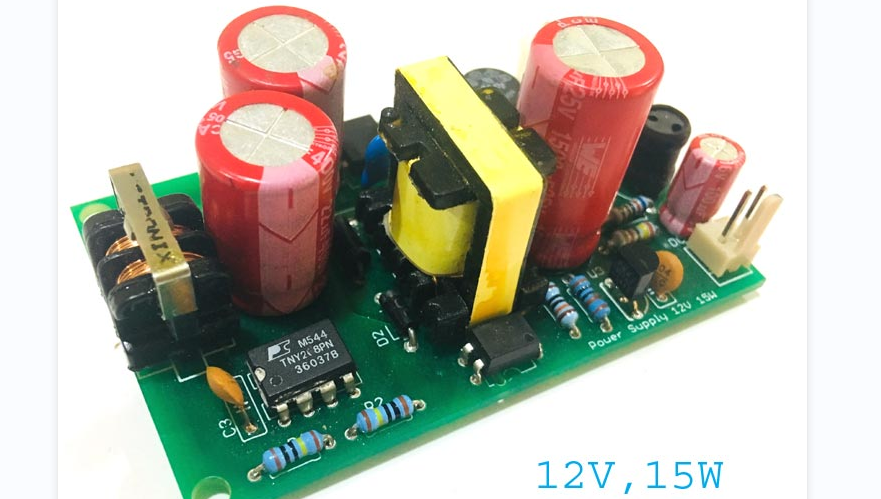
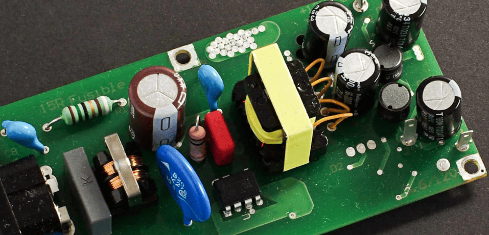
Power electronics PCB design is a crucial aspect of modern electronics engineering. It involves designing printed circuit boards (PCBs) that can handle high power levels and current densities, while also providing efficient and reliable performance. Power electronics PCBs are used in a wide range of applications, from power supplies and inverters to motor drives and renewable energy systems.
One of the main challenges in power electronics PCB design is managing heat dissipation. High power levels can cause significant heating, which can degrade performance and reliability if not managed properly. To address this challenge, designers must carefully consider factors such as thermal conductivity, component placement, and PCB layout. They may also use techniques such as heatsinking, thermal vias, and thermal management software to optimize heat dissipation and ensure reliable operation.
Basics of Power Electronics PCB Design
Understanding Power Electronics PCBs
Power electronics PCBs are designed to handle high voltage and current levels, making them suitable for use in power electronic circuits. The design of these boards is critical in ensuring that the circuit operates efficiently and reliably. Power electronics PCBs are typically designed with a few key considerations in mind:
- Heat dissipation: Power electronics circuits generate a lot of heat, so the board must be designed to dissipate this heat effectively.
- High voltage and current: The board must be designed to handle high voltage and current levels without failing or causing damage to other components in the circuit.
- Noise eduction: Power electronics circuits can be noisy, so the board must be designed to minimize noise and interference.
Layout Techniques for Power Electronics PCBs
When designing a power electronics PCB, it is important to consider the layout of the board. Some key techniques to keep in mind include:
- Separating high and low voltage circuits: High voltage and low voltage circuits should be physically separated on the board to prevent interference between the two.
- Minimizing trace length: Longer traces can increase resistance and reduce efficiency, so it is important to keep trace lengths as short as possible.
- Placing components strategically: Components should be placed in a way that minimizes noise and interference and maximizes heat dissipation.
Component Selection for Power Electronics PCBs
Selecting the right components is critical for the design of a power electronics PCB. Some key considerations when selecting components include:
- Voltage and current ratings: Components must be able to handle the voltage and current levels used in the circuit.
- Temperature rating: Components must be able to withstand the high temperatures generated by the circuit.
- Efficiency: Components should be selected for their efficiency to ensure that the circuit operates as efficiently as possible.
Overall, designing a power electronics PCB requires careful consideration of a range of factors, including heat dissipation, high voltage and current levels, noise reduction, layout techniques, and component selection. By taking these factors into account, designers can create PCBs that are reliable, efficient, and effective for use in power electronics circuits.

Advanced Techniques for Power Electronics PCB Design
When designing power electronics PCBs, there are several advanced techniques that can be employed to ensure optimal performance and reliability. These techniques include thermal management, EMI/EMC considerations, and high-frequency design techniques.
Thermal Management for Power Electronics PCBs
Thermal management is critical in power electronics PCB design, as excessive heat can lead to component failure and reduced lifespan. To mitigate these risks, designers can incorporate a range of techniques, including:
- Heat sinks: These are passive cooling devices that absorb and dissipate heat from hot components, such as power transistors and diodes.
- Thermal vias: These are small holes drilled into the PCB that allow heat to dissipate from one layer to another.
- Copper pours: These are large areas of copper on the PCB that act as a heat sink, absorbing and dissipating heat from components.
- Thermal pads: These are copper pads placed under components, providing a direct thermal path to the PCB.
EMI/EMC Considerations for Power Electronics PCBs
EMI/EMC (electromagnetic interference/electromagnetic compatibility) considerations are important in power electronics PCB design, as these circuits can generate significant electromagnetic noise that can interfere with other circuits and devices. To minimize EMI/EMC issues, designers can employ a range of techniques, including:
- Ground planes: These are large areas of copper on the PCB that act as a shield, preventing electromagnetic noise from escaping the circuit.
- Shielding: This involves placing conductive material, such as metal foil, around sensitive components or circuits to prevent electromagnetic noise from entering or leaving.
- Filtering: This involves using passive components, such as capacitors and inductors, to filter out unwanted electromagnetic noise.
High-Frequency Design Techniques for Power Electronics PCBs
High-frequency design techniques are important in power electronics PCB design, as these circuits often operate at high frequencies that can lead to signal degradation and other issues. To ensure optimal performance, designers can employ a range of techniques, including:
- Impedance matching: This involves ensuring that the impedance of the circuit matches the impedance of the load, minimizing signal reflection and distortion.
- Controlled impedance: This involves ensuring that the impedance of the PCB traces is consistent throughout the circuit, minimizing signal degradation.
- Differential signaling: This involves using two traces to transmit a signal, minimizing noise and interference.
By incorporating these advanced techniques into their power electronics PCB designs, designers can ensure optimal performance, reliability, and longevity.
Testing and Validation of Power Electronics PCBs
Power electronics PCBs are critical components of many electronic systems, and their performance and reliability are essential for the overall system’s success. Testing and validation of power electronics PCBs are crucial steps in ensuring that the PCBs meet the required performance and reliability specifications.

Functional Testing of Power Electronics PCBs
Functional testing of power electronics PCBs involves verifying that the PCB performs its intended function correctly. This testing may include testing the power supply, voltage regulation, current handling, and other functions. Functional testing can be done using test equipment such as oscilloscopes, power supplies, and signal generators.
Environmental Testing of Power Electronics PCBs
Environmental testing of power electronics PCBs involves subjecting the PCBs to various environmental conditions to verify their resistance to environmental factors. This testing may include temperature cycling, humidity testing, vibration testing, and shock testing. Environmental testing can help identify potential issues that may arise due to exposure to harsh environmental conditions.
Validation of Power Electronics PCBs
Validation of power electronics PCBs involves verifying that the PCB meets the required performance and reliability specifications. Validation testing may include testing for compliance with industry standards, such as IPC standards. Validation testing can also include testing for electromagnetic compatibility (EMC) and electromagnetic interference (EMI).
In summary, testing and validation of power electronics PCBs are crucial steps in ensuring that the PCBs meet the required performance and reliability specifications. Functional testing, environmental testing, and validation testing are essential components of the testing and validation process. By performing these tests, engineers can identify potential issues and ensure that the PCBs meet the required specifications.
Future Trends in Power Electronics PCB Design

Emerging Technologies in Power Electronics PCB Design
The field of power electronics PCB design is constantly evolving, and several emerging technologies are expected to shape its future. Some of these technologies include:
- Wide Bandgap Semiconductors: Wide bandgap semiconductors such as silicon carbide (SiC) and gallium nitride (GaN) are becoming increasingly popular in power electronics PCB design due to their superior performance and efficiency compared to traditional silicon-based semiconductors.
- Smart Power Modules: Smart power modules (SPMs) integrate multiple power components such as MOSFETs, IGBTs, and gate drivers in a single package, simplifying the design process and reducing the size of power electronics PCBs.
- 3D Printing: 3D printing technology can be used to create complex and customized power electronics PCBs with high precision and accuracy, reducing the need for manual assembly and improving the overall performance of the PCB.
Challenges and Opportunities in Power Electronics PCB Design
While there are several emerging technologies in power electronics PCB design, there are also several challenges that must be addressed. Some of these challenges include:
- Thermal Management: Power electronics PCBs generate a significant amount of heat, and effective thermal management is critical to ensure the reliability and longevity of the PCB.
- Size and Weight Reduction: Power electronics PCBs are often large and heavy, making them unsuitable for certain applications. There is a growing demand for smaller and lighter PCBs that can be used in portable devices and other compact applications.
- Cost Reduction: Power electronics PCBs can be expensive to manufacture due to the use of specialized components and materials. There is a need to reduce the cost of power electronics PCBs while maintaining their performance and reliability.
Despite these challenges, there are also several opportunities in power electronics PCB design. For example, the increasing demand for renewable energy sources such as solar and wind power is driving the need for more efficient and reliable power electronics PCBs. Additionally, the growing popularity of electric vehicles and other electrified transportation systems is creating new opportunities for power electronics PCB designers.
Comments are closed