A lot of work goes into the fabrication and the assembly of Printed Circuit Boards (PCBs). For people who may not be conversant with how the two processes work, we have put together some helpful tips to help you in understanding how each of these important PCB techniques works.
What Is PCB Fabrication?
It is important to explain each of these PCB processes so that you will understand how they work. The first is the PCB Fab.
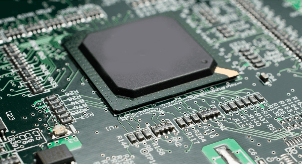
What is PCB Fab? PCB Fab, which is the short form of Printed Circuit Board (PCB) Fabrication, is a specific method of assembling the components and the properties of a Printed Circuit Board (PCB).
This assembly is specifically for the manufacturing of PCBs, which are mainly used in computer and electronic devices.
Ideally, the layers of the Printed Circuit Boards (PCBs) will be put together alongside the surface pattern. This will later be used in the manufacturing of electronics.
————————————————————-
Request PCB Manufacturing & Assembly Quote, Pls Send PCB File to Sales@raypcb.com Now
————————————————————-
Important Steps in PCB Fabrication
The fabrication of Printed Circuit Boards (PCBs) doesn’t come easy. Many processes and steps have to be taken before you can successfully get it done.
We understand the importance of mastering these processes, as they are beneficial when you want to produce reliable Printed Circuit Boards (PCBs).
Read on to find out the various steps in this ultimate guide to PCB Fabrication.
- PCB Layout
The design or the layout of the Printed Circuit Boards (PCBs) should be paramount. It is only when you have a general outlook (layout) of the boards that you can be able to proceed with the fabrication.
In this case, you are looking at connecting the different elements, as well as widening the routes, and placing vias on the different sizes that they match.
There are more things to the fabrication of Printed Circuit Boards (PCBs). We have explained those below.
- Software Selection
The software plays an important role in the outcome of the PCB design. With many software versions out there, you may not be sure of the one to use.
We advise that you stick to the primary software that is common in the PCB industry. These are the Eagle, Altium Designer, KiCad, OrCAD, and Pads.
- Gerber Files
Many PCB manufacturers allow you to upload your Gerber Files. These files are the expected outcomes you want to have at the end of the PCB fabrication and assembly. With that in mind, the PCB manufacturer will set about the task of working to meet up with your expectations.
Having said that, we also need to consider other important aspects of the Gerber Files. The Gerber files have specific information and requirements that must be met.
This ranges from the Component Notations, the Copper Tracking Layers, the Apertures, and the Drill Drawing.
Aside from those, here are the other necessary files that need to be in place before a Printed Circuit Board (PCB) can be manufactured.
- Paste layers
- Solder mask
- One or more fabrication drawings
- An accurate outline that shows the slots and cutouts on the PCBs
- A drill file (with the Excellon format ASCII) should be used for each cycle.
- Tool codes for the drill files
- Review
The Gerber files and other related documents will be sent to the PCB manufacturer through the dedicated channel. It could be posting it to the manufacturer’s office or uploading the Gerber files on the PCB manufacturer’s website.
Once the manufacturer acknowledges receipt of the Gerber files, the next step would be to submit the same to the engineer for review.
This pre-production engineering process helps in the discovery of likely missing documents and helps in running the necessary checks. The accurate quotation will also be given during this process.
At the end of it all, the quotation will be released and if you are okay with it, the production phase will be initiated.
- Pre-Production
Before the actual production of the PCB, some steps need to be taken.
First, cutting and lamination will be done. This will be centred on the size of the panel or the size of the finished board.
Second, the board will be dried. The aim is to prevent the board from warping during the production phase. It also helps to remove the moisture on the Printed Circuit Board (PCB).
Ideally, the drying process will be done for 4 hours at a temperature of 150 degrees centigrade.
- Inner Layer Imaging
The inner layer of the Printed Circuit Board (PCB) will pass through the imaging phase.
Here, a dry film (Inner Film) will be applied to the visible copper core board. Also, the necessary photo imaged reactions will be carried out on the dry film.
The next step is the Inner Exposure, where the core plate will be allowed to dry.
The third step here is to develop the inner layer (Inner Layer Development). In this case, the unexposed dry film will be developed to the point that the original copper skin is revealed. The exposed dry film will also be retained. On the other hand, the exposed core plate of the PCB will be developed too.
————————————————————-
Request PCB Manufacturing & Assembly Quote, Pls Send PCB File to Sales@raypcb.com Now
————————————————————-
- Etching the Inner Layer
The inner layer of the Printed Circuit Board (PCB) will also be etched. In the course of etching the line, there will be a protection of the copper skin that is covered by the dry film.
On the other hand, the copper skin, which has not been protected by the dry film, will be etched away.
Besides, if there is a need to retain any of the line patterns, such would be retained after it must have been displayed by the etching process.
If the line pattern must be fully retained, the dry film of the copper sheet on the main board must be treated.
- Automatic Optical Inspection
Here, the Automatic Optical Inspection (AOI) will be carried out on the inner layer of the Printed Circuit Board (PCB).
The aim of running the Automatic Optical Inspection (AOI) is to check the reliability of the etching. Here, the concentration is on finding out if the etching was clean or not. It also checks if the core plate of the PCB has an open or a short circuit after etching.
- Lamination
The lamination process has to do with the pressing of one board via the insulating medium called the “PP.”
- Drilling
The drilling process entails laminating the plate of the PCB. Because there is no metal on the hole of the board, the layers may not be connected.
- Hole Coating
A hole will be coated on the Printed Circuit Board (PCB) via a process called “Electroless Copper Deposition.”
This will be done via a chemical reaction and will require about 3um of very thin layered copper.
- Hole Thickening
The hole on the PCB will be thickened to 8um using the electron transfer reaction. It is important to mention that this will be actualized by using horizontal electrolytic plating on the copper in the hole and on the copper in the bare plate.
- Imaging the Outer Layer
The outer layer of the PCB will be imaged. Among the many processes involved here is the performing of photo imaged reactions on the dry film, the drilling of holes on the plate, as well as the application of the dry film to protect the hole on the plate.
The outer layer will also be exposed and later developed by etching the copper on the dry film.
- Graphic Plating
The copper that needs to be retained at the end/the bare copper will be thickened through the thick copper plating and the tin plating processes.
- Etching the Outer Layer
The outer layer of the copper will be etched by retaining the copper protecting the tin.
Also, the tin protecting the copper will be removed.
- Masking and Silkscreen
The entire panel of the PCB will be coated with the solder mask. After it must have been exposed to high-density UV light, the panel will not be susceptible to corrosion and oxidation.
The Silkscreen process will then come next. Here, the important information of the Printed Circuit Board (PCB) will be printed on it.
- Surface Finish
The Printed Circuit Board (PCB) will finally be passed onto the surface finishing and the coating processes.
The idea here is that the PCB will have better soldering and will have the surface protected.
- Profiling and Testing
The Printed Circuit Board (PCB) will be checked thoroughly for possible corrections. If none was found, it will be tested electrically to ensure that the board functions as expected.
- Final Inspection
There will be a Final Visual Inspection, where the quality control experts will inspect the PCB.
Some of the areas of inspection are:
- Warpage requirement
- Visual inspection
- Aperture hole number measurement
- Product size inspection
If the PCB scaled or passed the inspection, it will be designed a test report that shows the outcome of the inspection.
Wrapping Up
Once the Printed Circuit Board (PCB) has been confirmed to comply with the industry standards (and after it must have passed the tests), it will be packaged and delivered to the buyers.
We believe that you have now understood the basic processes involved in PCB Fabrication and Assembly.
When you are ready to go ahead with your PCB design, do well to look for the best PCB manufacturers who will offer you the best service.
Comments are closed