Every electronic gadget relies on PCBs. You can’t expect proper operation from the electrical gadget without it. The demand for PCBs will never end.
Many people like to do their own circuits work on printed circuit boards. The number of people interested in PCBs as a hobby is increasing. And more resources are needed to accommodate them. Happily, numerous free applications exist for simple PCB design. When constructing something more involved, however, you should hire an expert at a rate not much higher than the DIY options.
PCB Production for Hobbyists
PCB maker services from Candor are ideal if you need professional quality work at a hobbyist’s cost. We have the ability to generate high-quality products in a short amount of time. When you combine our personalized service with our streamlined production methods and high-quality, commercial-grade fabrication, you get everything a company offers at a hobbyist’s cost.
The open-hardware industry is one that Candor helps support. Our services for hobbyists are ideal whether you are just getting started, like to play around, or are plotting a project on a bigger scale.
Excellent Quality Components
You should not compromise for low-quality components because you are only making PCBs for fun. We guarantee the same high standard of service for both professional and amateur PCB projects.
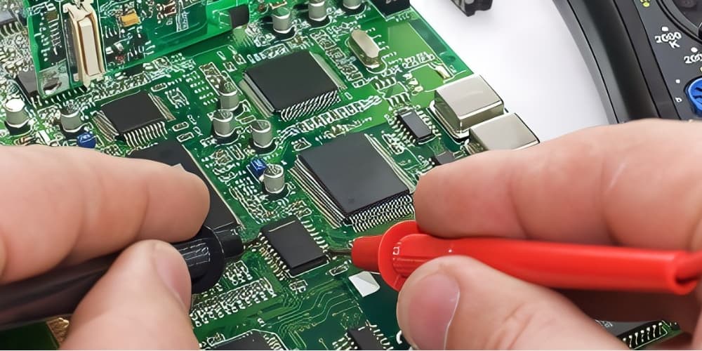
All fields can make use of the high-quality circuit boards we offer. PCB materials from Candor are top-notch in every respect, making them ideal for use in anything from medicine and aerospace to manufacturing and other commercial enterprises.
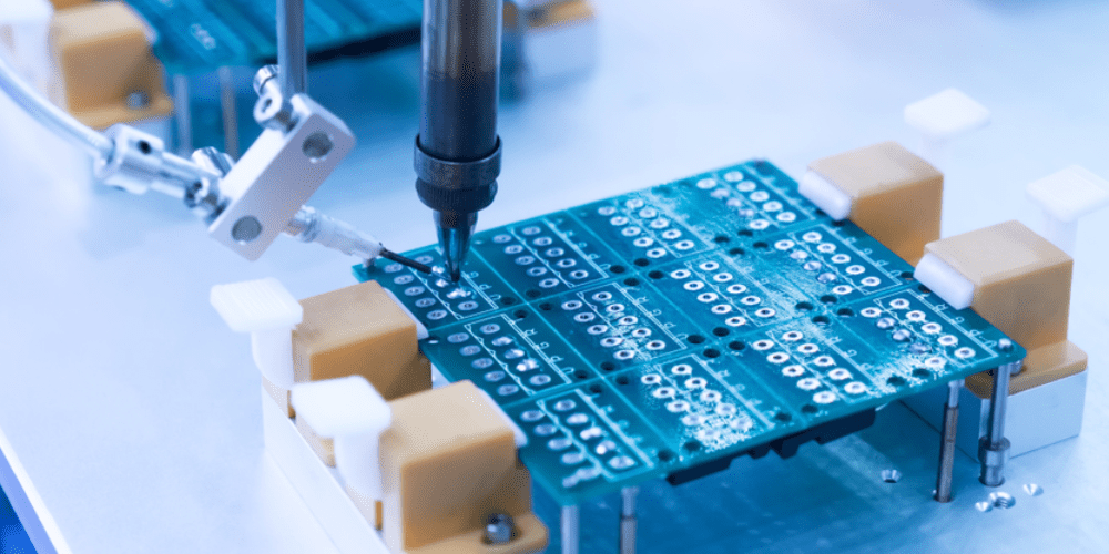
Prototyping at Rapid Speeds
You still need a fast turnaround period for your PCB, even when you’re doing it on the side as a hobby. The more you have to wait for your PCB maker, the less chance you have to make changes. We also guarantee lightning-fast delivery times for prototyping.
If you need a prototype PCB quickly, you can have one made in as little as twenty-four hours. Creating a prototype for a more difficult design can be as long as three days, while mass production can take up to ten.
Personal Attention to Each Client
Whether you’re running a business for a living or as a hobby, providing excellent customer care is essential to your success. Individualized attention gets provided by Candor’s staff all the way through the PCB design, prototyping, and production phases.
We guarantee prompt shipment. We’re pleased to say that our on-time delivery percentage exceeds 99 %. In all cases, regardless of the scope of the project or the nature of the client, we will do our best to meet the promised delivery date.
New Method for Streamlining Production
As a hobbyist, you probably want to avoid any complexity. You want a straightforward, cutting-edge production procedure even when you’re working with a complex design.
Our production philosophy is based on streamlining the production process while also being ecologically responsible, guaranteeing you the highest quality products possible and minimizing any disruption to your business. By utilizing less water than other methods and adhering to the principle of “reduce, recycle, and reuse,” our method is able to outperform all others.
Professional Standard Manufacturing
A hobbyist should be able to afford high-quality fabrication, just like a pro. Your interest now may become a career path in the future. We use the same high-quality solutions that we would provide to a commercial client throughout the entire production process. You’ll have full control over all of the cutting-edge processes, which will expand the potential of your PCB layout.
When it comes to satisfying our clients, Candor never stops looking for innovative solutions. Whether you’re an amateur designer or a professional. We want you to know that your work will get appreciation.
In the PCB industry, hobbyists can choose from a wide variety of board types to suit their needs.
They can have one, two, or even more layers. The number of foil sheets on a certain board is a determining factor. It’s worth noting that creating multilayer PCBs is a pretty straightforward task. Putting this together is as simple as gluing together some dielectric sheets. Furthermore, they differentiate between rigid and flexible boards.
Making your own printed circuit board has never been simpler.
There are two methods for producing PCBs at home: chemical and mechanical. In any event, you should get the tools and supplies you’ll need before you do anything else. Preparing the software has usage to make the drawing in order to use the cheapest technique of producing PCBs. In terms of simplicity, Sprint-Layout is the best option for newcomers.
The interface is straightforward, and hobbyists may use it for free if they make their own printed circuit boards. Foil fiberglass is by far the most available radio element, and there is a big library dedicated to it. It is a robust plastic laminate with a copper coating on one or even both faces. Typically distributed on a flat sheet.
Durable in harsh environmental conditions
Electronics hobbyists can find glass-fiber textolite for PCBs through specialized online retailers. Transparent polyethylene material, required to transfer the design from the display of a laptop or PC, should ideally be thicker for beginners, making it much simpler to deal with.
Use a rigid film (textbook covers are perfect for this) and sticky tape to attach it to the display. It is good to take a thin one because it is simpler to remove afterward. Drawings made on a computer screen can be easily transferred to HDPE using a standard felt-tip pen. However, a specific marker developed for use in making PCBs is the only way to go from the films to the foil textolite.
- Permanent pens (available at office supply stores) can also be used.
- Materials include sandpaper with a particle size of around 1000 to 1500 units.
- Ninety-six percent solution of ethyl alcohol (you may also apply nail polish cleaner).
- A toothbrush.
- Equipment for drilling holes of 0.7 to 1.2 mm diameter.
- An acrylic, plastic, or glass bowl for etching.
- A brush for applying paint.
A soldering iron and all the necessary equipment for soldering (liquid and solid flux); FeCl3 (although any mixture can be used for fabricating boards, such as a citric acid solution in H2O2 by a PCB producer catering to hobbyists); and paint all need to get purchased separately.
Step-by-Step Methodology
The manufacturing procedure for a homemade PCB can begin once all the necessary materials get assembled.
Phase 1:
First, either make a design from scratch using dedicated software (if your idea is truly one of a kind) or get a ready-made one from the web. Get the image off the screen and onto the plastic. After attaching it to the screen, you can draw the conducting paths and contact areas with a special pen.
Phase 2:
This stage focuses on getting the foil fiberglass ready. You can use a hacksaw or metal cutters, an engraving, or just a regular kitchen knife to cut a sufficient size. As a next step, sandpaper should be used to remove the protective layer from the surface layer of the copper.
Leaving the scratches made with the sandpaper grains on the fiberglass could improve future adhesion, so it’s not a bad idea to leave them there. Using alcohol or a varnish cleaner, clean the surface of the workpiece of any leftover dust after stripping.
Phase 3:
There will be a requirement to transfer polyethylene and the corresponding PCB templates to fiberglass. In order to achieve this, PCB makers dedicated to hobbyists must first tape the screen on the prepared particles before drilling holes in accordance with the indications. Straight polyethylene pipe will allow this. When the project calls for a new hole size, it’s important to swap out the drill bits as soon as possible.
Phase 4:
Take it out of the plastic and set it aside to cool after the drilling of the openings. You must now use permanent pens to design potential conductive paths. Having a variety of pens on hand that can produce lines of varying thicknesses is preferable.
PCBs for home use can get drawn by tracing a template onto polyethylene or by viewing the original on a monitor. The lines should get drawn with a single stroke to avoid having to make any alterations (the pattern from the permanent pen is badly removed). The pattern you just painted needs time to cure.
Phase 5:
The fifth phase is to mix up some etching solutions for the PCBs. To employ ferric chloride, water and dry powder are combined in a non-metallic mixing vessel. You can create a solution a bit stronger than what’s called for on the packaging to speed things up if you like.
The chemical process can be sped up by placing the container containing the solution in a tub of heated water, and the etching process can get completed in 10 minutes rather than the recommended 60. Brushing the reaction byproducts off the board requires continual, modest movement in the solution.
Phase 6:
After cleaning the piece properly under clean water, all traces of the pens get removed with alcohol or nail polish cleaner. As the last step, after cleaning, the PCB needs to get patted dry.
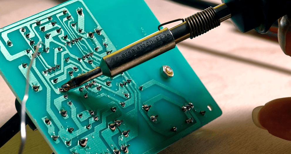
Phase 7:
Phase 7 involves in-house tinning of the board. At first, you can use sandpaper to polish the surface once more, this time with greater care. The next step is to wet the prepared paths with liquid flux and preheat a soldering gun. After soldering the etched copper, the etching process is complete. You must get the conductive channels nice and hot for this to work.
Chemical tinning of PCBs is possible with liquid tin, which makes the process easier, or with Rose or Wood alloys. Unlike the former, the latter doesn’t lump when it’s spread down the routes.
You can observe that even a beginner radio hobbyist has the ability to make PCBs without spending too much money on the process. It will be feasible to produce electronics that are competitive with factory-made options using the suggested technologies and existing materials.
How to Manufacture a Hobbyists PCB with DIY Procedures?
Technique 1:
- Prepare the copper-clad laminates for PCB manufacture by cutting them to the correct dimensions.
- Place the stencil paper on a metal plate and make the drawing of the circuit model using a pen (the diagram’s scale must be one ratio one). The stencil is then cut down to the appropriate size for the PCB and pasted onto the copper-clad lamination. Make an appropriate printing substance by mixing a little talcum powder and paint together, dipping a paintbrush in the material, and applying it evenly on a sheet of stencil paper. It should be said multiple times. The printed board can then be used to print the circuit. The printed board is reusable and great for making a few units at a time.
- To corrode the printed circuit board, mix together one gram of KClO3 and forty milliliters of HCl at a 15 percent concentration to make a corrosive solution.
- To remove corrosion from printed boards, simply wash them with water over and over again. Use banana oil to remove the paint, and then wash the board thoroughly so that no corrosive residue gets left behind when you print on it. Using a rosin mixture, cover the area. Do not drill until it has dried.

Technique 2:
- Components should have a position and density determined by the basic schematic drawing and the dimensions of the PCB area. The placement of the parts should follow the “big first, little later” rule, which states that global or system-level considerations should take precedence over local ones. The circuit’s components are all close together and evenly spaced.
- Intersections or corners of two tracks are not usable for bending the connected trace between parts at a straight angle. They have to make a turn together and can’t cross each other too much. In cases where this is not possible, the printed circuit can be moved to the rear of the PCB and connected to the front side by stud screws. Alternatively, you might use shielded traces when connecting the components.
- It’s preferable to put some space between the input and output components so that they don’t accidentally interact with one another.
Comments are closed