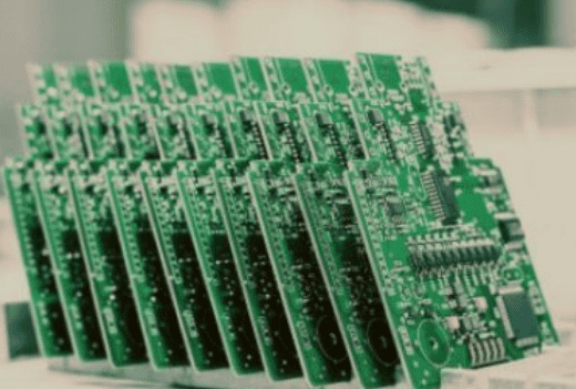
Printed circuit boards are the lifeline of all machines. That’s why they need to perform well.
You may hear the designers focus on EMC PCB in PCB design. EMC stands for electromagnetic compatibility. Designers greatly focus on it while designing any PCB design. Actually, a good PCB design improves the EMC and reduces the EMI. Several things have to be kept in consideration while designing the best EMC PCB design. Let’s dig deeper to learn about the EMC PCB design and how adenine can improve EMC performance.
What are EMC and EMI?
EMC in a PCB shows the board’s capability of working in its electromagnetic environment. Better EMC means it doesn’t emit awful electromagnetic interference. It means there is less or no noise. EMI stands for electromagnetic interference. It is the second name for electromagnetic noise. Simply put, it is a disturbance of electromagnetic waves to one device from another. That’s why every PCB designer tries to follow the best practices and standards for EMC. In this way, they can reduce the EMI and its negative effects. So EMC testing is necessary before finalizing the design.

Guideline for EMC PCB design to reduce the EMI
The following guidelines will help you to design the best-printed circuit boards according to Industry practice. Undoubtedly, the design of printed circuit boards plays an important role in EMC performance. Keep the following thing in mind while designing PCBs.
Focus on the ground planes.
Almost every printed circuit board has ground planes. The sole purpose of this ground plane is to reduce noise and interference. Focusing on better materials for ground planes and intelligent design can help to reduce EMI. Ground planes can contribute to enhancing the EMC. In multi-layer PCBs, it’s tricky to handle the ground planes, but gridding the ground reduces EMI radiation from the signal traces. Gridding is successful in improving EMC performance even in two-layered PCBs.
Protective components can do wonders.
Sometimes electric voltage difference, power disruption, and electric shock can contribute to the EMI. So avoiding all these transient voltage suppressor diodes can help you while designing PCB. Keep in mind the placement of such components.
Arrange the parts smartly
Electronic parts and their placement play an important role in printed circuit board construction. Their wrong placement can result in EMI. So it is necessary to place the components smartly on the board to improve. EMC. PCB zoning can also help you to improve EMC and general noise.
PCB zoning is a process of defining the general location of the component before any traces are set down.
Frequency signals
Planning the areas of the board in this way can have a major impact on the EMC performance of the PCB. Controlling the length of signals can help in this matter. Sometimes it doesn’t help, so designs have to look for other ways to improve EMC performance.
Choose modern PCB designing tools.
Nowadays, many advanced PCB designing tools are available in the market. These PCB designing tools have many inbuilt functions. In this way, you can design the best PCB with the best EMC. Different high-end software also helps in the intelligent placement of parts. As a result, you have improved EMC and better performance. Now it’s up to the designers how intelligently they use these tools and save their time.

Some additional tips for EMC PCB design
- Pay attention to the oscillator’s position while designing PCB. Don’t place oscillator tank loops near the analog circuits.
- Keep high noise lines away from the edge of the PCB. In this way, it doesn’t disturb the other components’ functions.
- Cable assemblies and their placement is another reason for the noise. Because these assemblies can pick up the noise easily and degrade the EMC performance, so focus on their placement also.
- Follow the industry practices and standards for EMC to avoid any future inconvenience.
EMC testing and why it is necessary
You undoubtedly spent a lot of time designing PCB and following all the instructions. You did very well. Sometimes designers ignore the EMC testing due to their overconfidence or due to any other reason. That’s a wrong practice. EMC testing will help you a lot to improve your final product. It gives you a chance to improve your PCBS by eliminating the flaws.
Following are some good reasons to show that why your boards should undergo testing for EMC;
For Safety purposes
EMC testing while designing circuit boards is necessary from a safety point of view. EMC testing ensures the safety of both the user and the operator. Sometimes ignoring the EMC testing can lead to some serious losses.
To check the Reliability
The designer always ensures that their circuit boards work efficiently. EMC testing lets the designer know whether their PCBs will work as they intended. Do environmental factors affect their efficiency or not? This testing also helps to know whether your designed PCB can meet its operational objectives or not. So EMC testing is a useful technique to find the flaws at the initial stage.
Standard practice
Still, many designers ignore the importance of EMC testing, but later they regret it. EMC testing is standard and mandatory. There are different regulations and standards according to the country and industry for which PCB is designed. . To comply with the laws, a designer must go for EMC testing. If you don’t comply with industry practice, it means these PCBc are not usable. So it is necessary to go for EMC testing and follow the industry standards.
Wrapping up the things
EMC testing is a crucial step in checking the Reliability and functionality of the PCB. You can avoid different EMC issues by opting for the best PCB design. If you choose the right design appropriate to the device, then you can save time and money. If you neglect the design faults later, you have to spend more time on investigation and re-design. PCB design for EMC is, therefore, one of the keys to a successful design. Keep in mind the following tips and tricks in mind to design the best EMC PCB design.
Comments are closed